

方案详情文
智能文字提取功能测试中
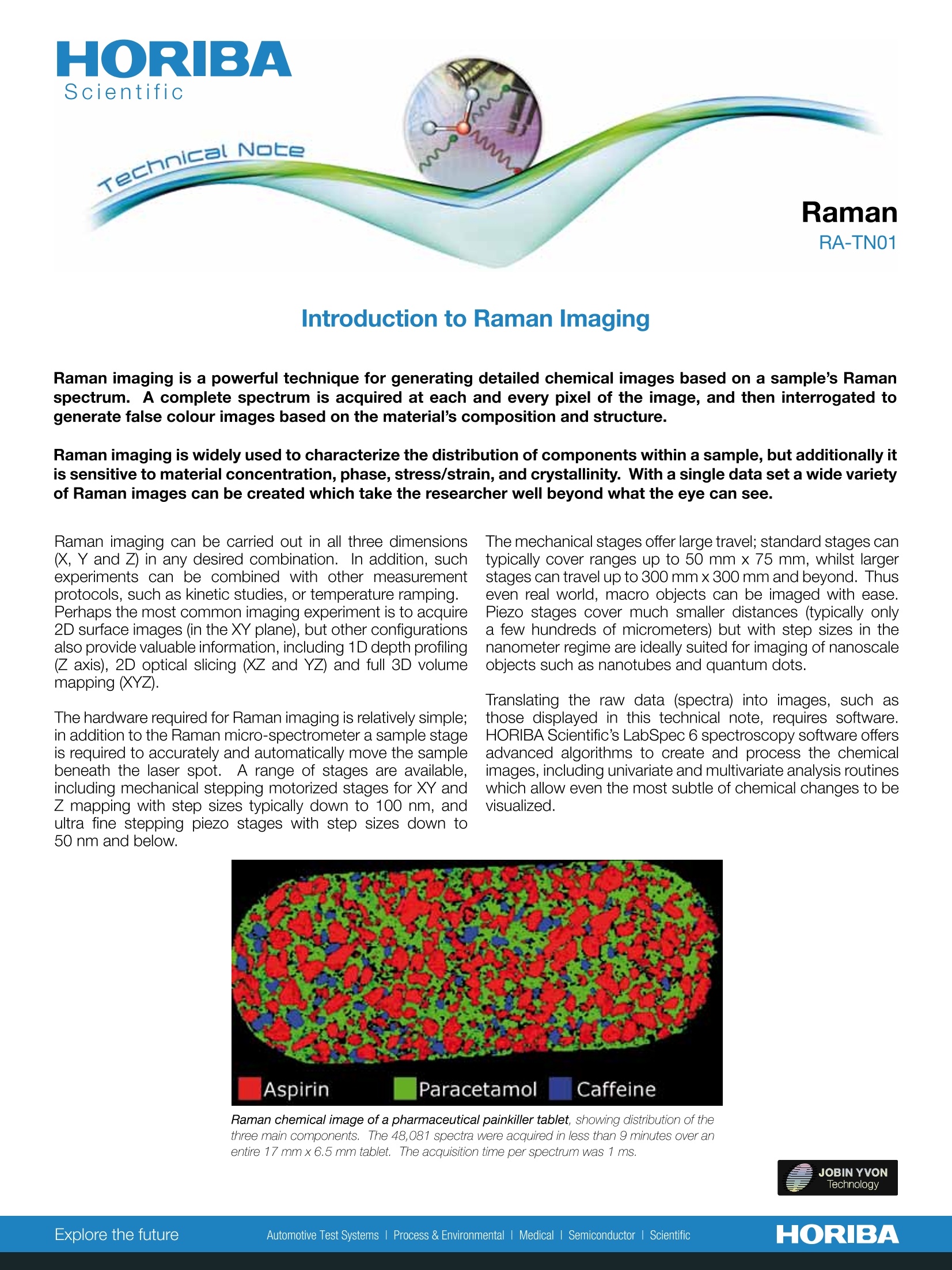
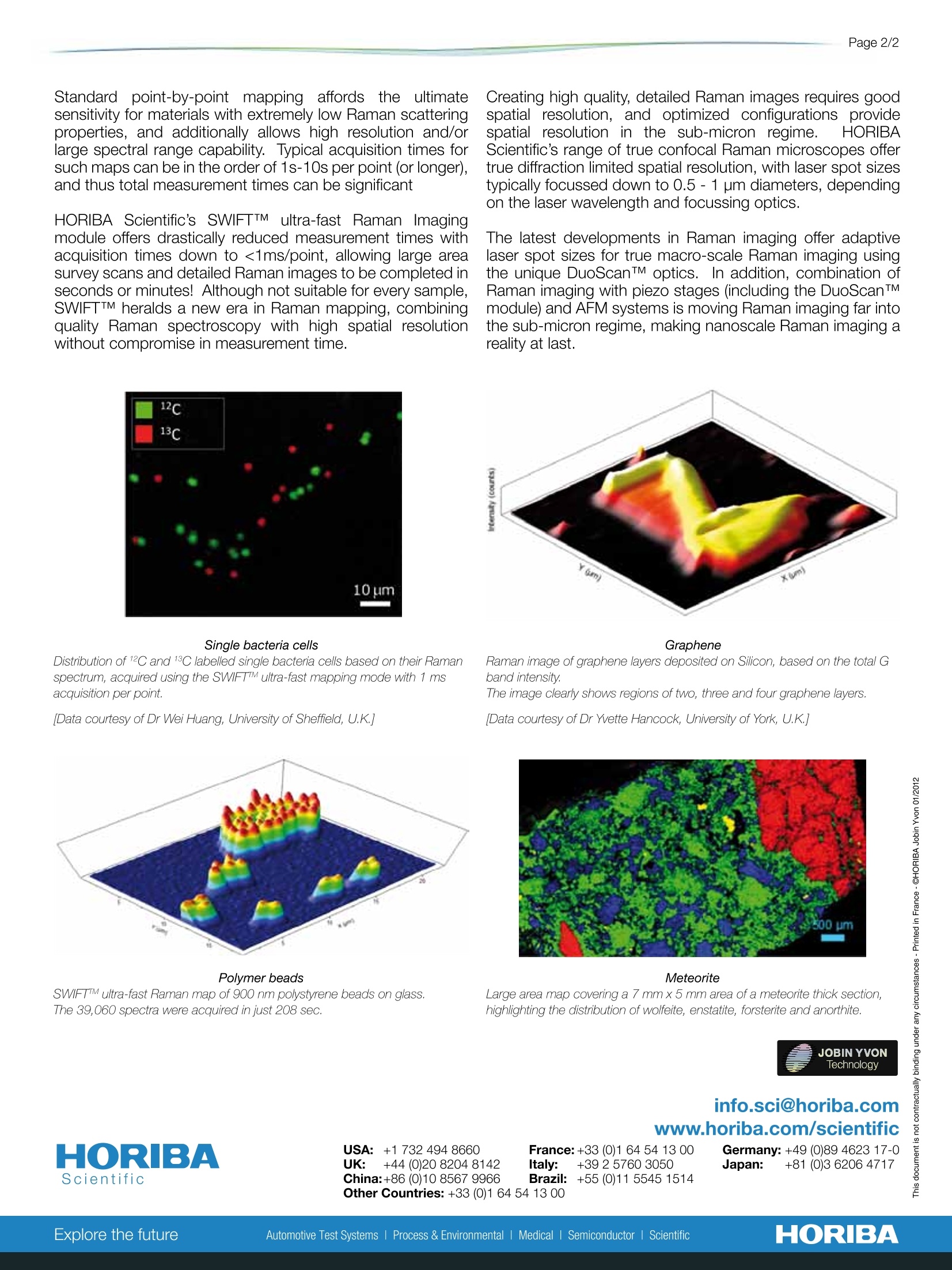
Page 2/2USA:+1 732 4948660UK:+44 (0)20 8204 8142China:+86 (0)10 8567 9966 Introduction to Raman Imaging Raman imaging is a powerful technique for generating detailed chemical images based on a sample’s Ramanspectrum. A complete spectrum is acquired at each and every pixel of the image, and then interrogated togenerate false colour images based on the material's composition and structure. Raman imaging is widely used to characterize the distribution of components within a sample, but additionally itis sensitive to material concentration, phase,stress/strain, and crystallinity. With a single data set a wide varietyof Raman images can be created which take the researcher well beyond what the eye can see. Raman imaging can be carried out in all three dimensions(X, Y and Z) in any desired combination. In addition, suchexperiments can be combined with other measurementprotocols, such as kinetic studies, or temperature ramping.Perhaps the most common imaging experiment is to acquire2D surface images (in the XY plane), but other configurationsalso provide valuable information, including 1D depth profiling(Z axis), 2D optical slicing (XZ and YZ) and full 3D volumemapping (XYZ). The hardware required for Raman imaging is relatively simple;in addition to the Raman micro-spectrometer a sample stageis required to accurately and automatically move the samplebeneath the laser spot. A range of stages are available,including mechanical stepping motorized stages for XY andZ mapping with step sizes typically down to 100 nm, andultra fine stepping piezo stages with step sizes down to50 nm and below. The mechanical stages offer large travel; standard stages cantypically cover ranges up to 50 mm x 75 mm, whilst largerstages can travel up to 300 mmx 300 mm and beyond. Thuseven real world, macro objects can be imaged with ease.Piezo stages cover much smaller distances (typically onlya few hundreds of micrometers) but with step sizes in thenanometer regime are ideally suited for imaging of nanoscaleobjects such as nanotubes and quantum dots. Translating the raw data (spectra) into images, such asthose displayed in this technical note, requires software.HORIBA Scientific's LabSpec 6 spectroscopy software offersadvanced algorithms to create and process the chemicalimages, including univariate and multivariate analysis routineswhich allow even the most subtle of chemical changes to bevisualized. Raman chemical image of a pharmaceutical painkiller tablet, showing distribution of thethree main components.The 48,081 spectra were acquired in less than 9 minutes over anentire 17 mm x 6.5 mm tablet. The acquisition time per spectrum was 1 ms. Standard point-by-point mapping affordstheultimatesensitivity for materials with extremely low Raman scatteringproperties, and additionally allows high resolution and/orlarge spectral range capability.Typical acquisition times forsuch maps can be in the order of 1s-10s per point (or longer),and thus total measurement times can be significant HORIBA Scientific’s SWIFTTM ultra-fast Raman Imagingmodule offers drastically reduced measurement times withacquisition times down to <1ms/point, allowing large areasurvey scans and detailed Raman images to be completed inseconds or minutes! Although not suitable for every sample,SWIFTTM heralds a new era in Raman mapping, combiningquality Raman spectroscopy with high spatial resolutionwithout compromise in measurement time. Single bacteria cells Distribution of 12C and 13C labelled single bacteria cells based on their Ramanspectrum, acquired using the SWIFT'M ultra-fast mapping mode with 1 msacquisition per point. [Data courtesy of Dr Wei Huang, University of Sheffield, U.K.] Polymer beads SWIFT'M ultra-fast Raman map of 900 nm polystyrene beads on glass.The 39,060 spectra were acquired in just 208 sec. (Creating high quality, detailed Raman images requires goodspatial resolution, and optimized configurationsprovideSCspatial resolution in the sub-micron regime. HORIBAScientific's range of true confocal Raman microscopes offertrue diffraction limited spatial resolution, with laser spot sizestypically focussed down to 0.5 -1 pm diameters, dependingon the laser wavelength and focussing optics. The latest developments in Raman imaging offer adaptivelaser spot sizes for true macro-scale Raman imaging usingthe unique DuoScanTM optics. In addition, combination ofRaman imaging with piezo stages (including the DuoScanTMmodule) and AFM systems is moving Raman imaging far intothe sub-micron regime, making nanoscale Raman imaging areality at last. Graphene Raman image of graphene layers deposited on Silicon, based on the total Gband intensity. The image clearly shows regions of two, three and four graphene layers. [Data courtesy of Dr Yvette Hancock, University of York, U.K. j Meteorite Large area map covering a 7 mmx5 mm area of a meteorite thick section,highlighting the distribution of wolfeite, enstatite, forsterite and anorthite. JOBINYVONTechnology info.sci@horiba.comwww.horiba.com/scientific HORIBAExplore the futureAutomotive Test Systems Process & Environmental Medical Semiconductor lIScientific
关闭-
1/2
-
2/2
产品配置单
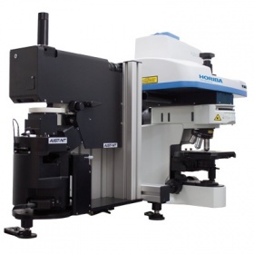
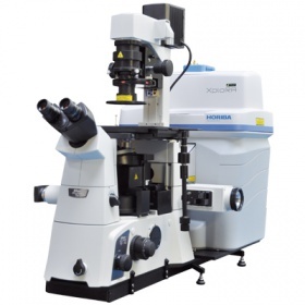
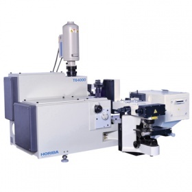
上海巨纳科技有限公司为您提供《Introduction to Raman Imaging》,该方案主要用于中检测,参考标准《暂无》,《Introduction to Raman Imaging》用到的仪器有HORIBAXploRA INV智能型全自动拉曼光谱仪、HORIBA HR Evolution高分辨拉曼光谱仪、HORIBACombiscopeXploRA原子力拉曼联用系统、Horiba XploRA INV 多功能拉曼及成像光谱仪、HORIBA T64000三级拉曼光谱仪。
我要纠错
推荐专场
激光拉曼光谱(RAMAN)
更多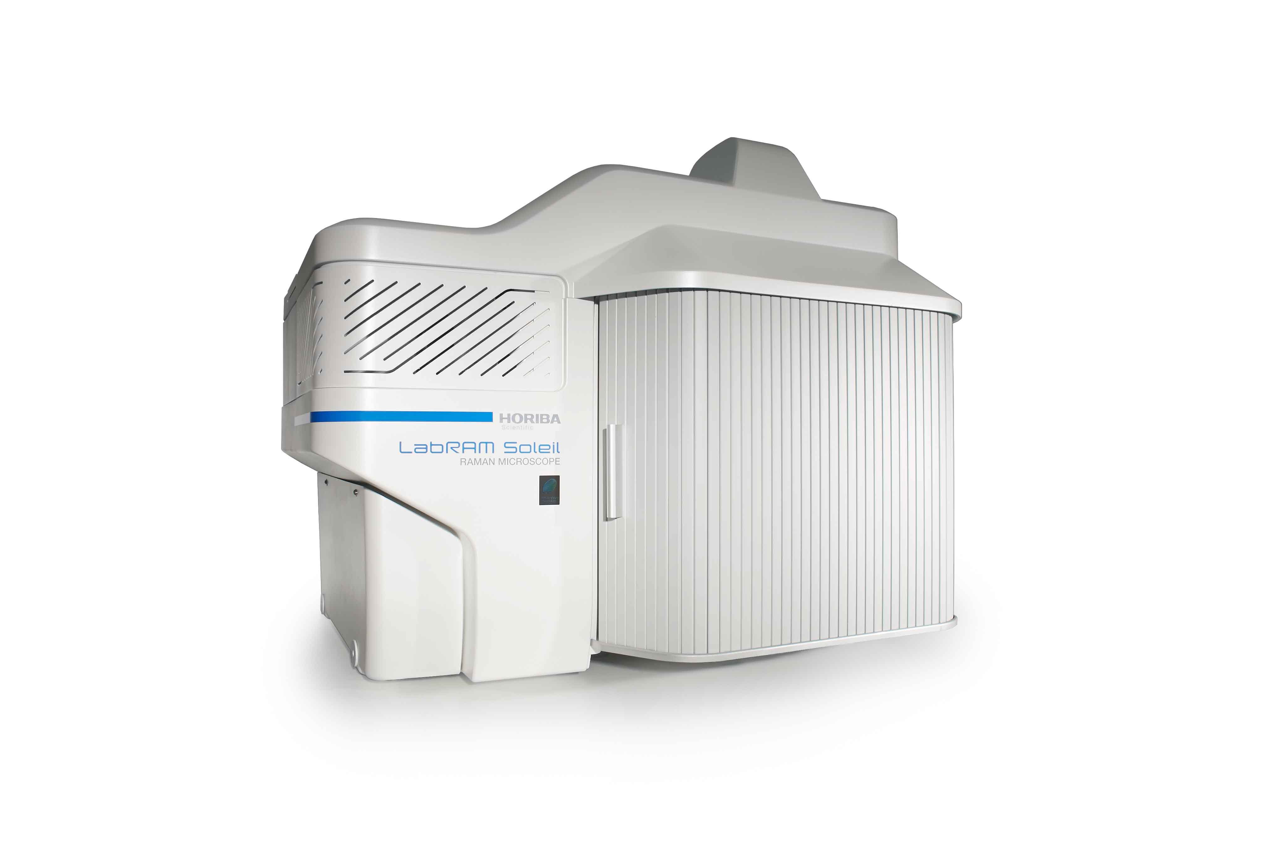
相关方案
 咨询
咨询