


您还有0次抽奖机会
锤子
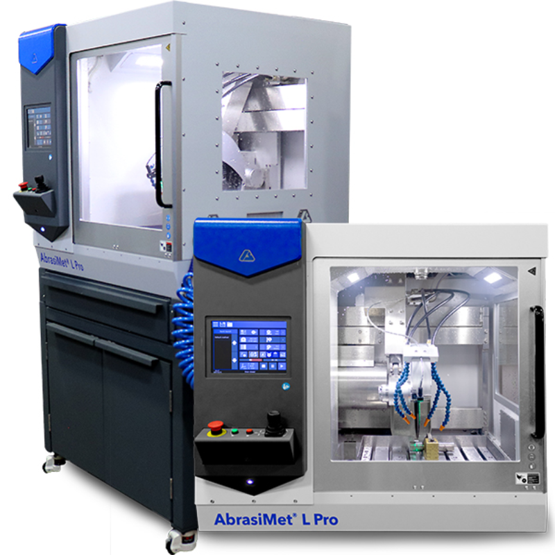
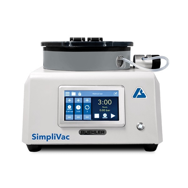
Microelectronics, Part I: Cutting, Mounting Written by: Scott Holt,Applications Engineer,Buehler Editor:George Vander VoortDirector, Research and Technology, Buehler Introduction For most microelectronic devices and packages, direct microscopic observation of a cross section is an important means of inspecting a particular defect. The creation of a cross section, as a destructive measure, is often used in the microelectronics lab as a decisive and final inspection tool after all other economical means of nondestructive inspection are employed. In order to produce a cross section, many of the techniques used in the metals industry have been borrowed; to a large degree, with success. However, the philosophy and logic for choosing a particular method of cutting, mounting, and abrasive preparation has often been lost in the process. This is of extreme significance because the needs of the microelectronics industry vary greatly from those of the metals industry. Issues such as feature size, specific area cross sectioning, and the ability to prepare a variety of materials with different mechanical properties within a single plane of polish require an understanding of basic abrasive processes so that appropriate sectioning methods might be developed. This issue of TECH-NOTES is the first half of a two part effort to summarize some of the basic concepts involved in proper preparation of microelectronic materials. We will discuss some simple guidelines which the microelectronic materials analyst might draw upon in the development of better preparation techniques. In particular, this issue will cover the variables involved in cutting and mounting of microelectronic materials, and summarize some of the technique and consumable choices that must be considered in order to achieve quality results. The next microelectronics issue of TECH-NOTES will continue with the abrasive processes of grinding and polishing these materials.
打开失败或需在电脑查看,请在电脑上的资料中心栏目,点击"我的下载"。建议使用手机自带浏览器。
