方案摘要
方案下载| 应用领域 | 电子/电气 |
| 检测样本 | 电子元器件产品 |
| 检测项目 | |
| 参考标准 | 无需 |
Microelectronics, Part I: Cutting, Mounting Written by: Scott Holt,Applications Engineer,Buehler Editor:George Vander VoortDirector, Research and Technology, Buehler Introduction For most microelectronic devices and packages, direct microscopic observation of a cross section is an important means of inspecting a particular defect. The creation of a cross section, as a destructive measure, is often used in the microelectronics lab as a decisive and final inspection tool after all other economical means of nondestructive inspection are employed. In order to produce a cross section, many of the techniques used in the metals industry have been borrowed; to a large degree, with success. However, the philosophy and logic for choosing a particular method of cutting, mounting, and abrasive preparation has often been lost in the process. This is of extreme significance because the needs of the microelectronics industry vary greatly from those of the metals industry. Issues such as feature size, specific area cross sectioning, and the ability to prepare a variety of materials with different mechanical properties within a single plane of polish require an understanding of basic abrasive processes so that appropriate sectioning methods might be developed. This issue of TECH-NOTES is the first half of a two part effort to summarize some of the basic concepts involved in proper preparation of microelectronic materials. We will discuss some simple guidelines which the microelectronic materials analyst might draw upon in the development of better preparation techniques. In particular, this issue will cover the variables involved in cutting and mounting of microelectronic materials, and summarize some of the technique and consumable choices that must be considered in order to achieve quality results. The next microelectronics issue of TECH-NOTES will continue with the abrasive processes of grinding and polishing these materials.

Introduction
For most microelectronic devices and packages, direct microscopic observation of a cross section is an important means of inspecting a particular defect. The creation of a cross section, as a destructive measure, is often used in the microelectronics lab as a decisive and final inspection tool after all other economical means of nondestructive inspection are employed.
In order to produce a cross section, many of the techniques used in the metals industry have been borrowed; to a large degree, with success. However, the philosophy and logic for choosing a particular method of cutting, mounting, and abrasive preparation has often been lost in the process. This is of extreme significance because the needs of the microelectronics industry vary greatly from those of the metals industry. Issues such as feature size, specific area cross sectioning, and the ability to prepare a variety of materials with different mechanical properties within a single plane of polish require an understanding of basic abrasive processes so that appropriate sectioning methods might be developed.
This issue of TECH-NOTES is the first half of a two part effort to summarize some of the basic concepts involved in proper preparation of microelectronic materials. We will discuss some simple guidelines which the microelectronic materials analyst might draw upon in the development of better preparation techniques. In particular, this issue will cover the variables involved in cutting and mounting of microelectronic materials, and summarize some of the technique and consumable choices that must be considered in order to achieve quality results. The next microelectronics issue of TECH-NOTES will continue with the abrasive processes of grinding and polishing these materials.
Specimen Preparation Philosophy
When considering preparation of a microelectronic device and/or package, the first step is to determine which materials are present in the cross section of interest. This is critical since these materials and their mechanical properties will determine, to a large degree, the course of action we take. Consider, for example, a small epoxy package in which we desire to cross section a silicon die and a gold ball bond near the die’s edge. If we were to encapsulate the package and grind to the edge of the die, (assuming the use of appropriate abrasives and technique), we might produce satisfactory results in a reasonable period of time.
This course of action would not be so easy, however, if the package were instead composed of ceramic. In this case, several choices present themselves. We can try to grind through the package, but we would, of course, require an aggressive grinding medium which may annihilate the brittle silicon upon contact. In addition to destroying the materials we plan to analyze, we would probably spend an inordinate amount of time (not to mention expense) getting to this point. A better option is to cut the package near to the plane of interest, using a precision diamond saw, and then to encapsulate the specimen for subsequent preparation.
The basic example above hints at a simple philosophy of preparation in which we carefully consider each stage of the process and it’s consequences towards the materials we choose to analyze. The following text summarizes basic cutting and encapsulation processes in order to promote a logical course of planning for microelectronic materials preparation.

标乐先进的制样技术-Mg及其合金制备
标乐先进的制样技术-汽车车身点焊样品制备
标乐先进的制样技术-片状多层陶瓷电容制样经验分析
相关产品
洛氏硬度计 RH2150 | 美国威尔逊硬度计 Wilson
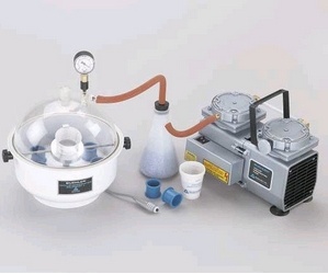
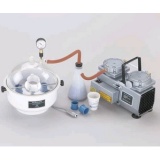
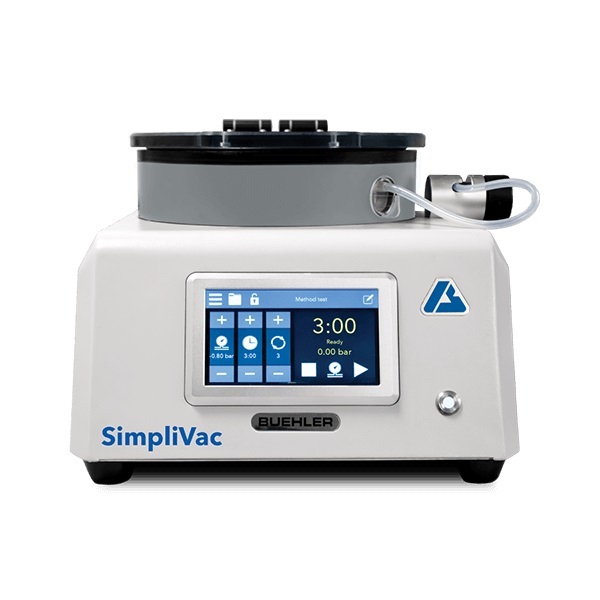
美国标乐 Buehler | SimpliVac 真空镶嵌机
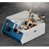
美国标乐 Buehler | AbrasiMet M 手动砂轮切割机
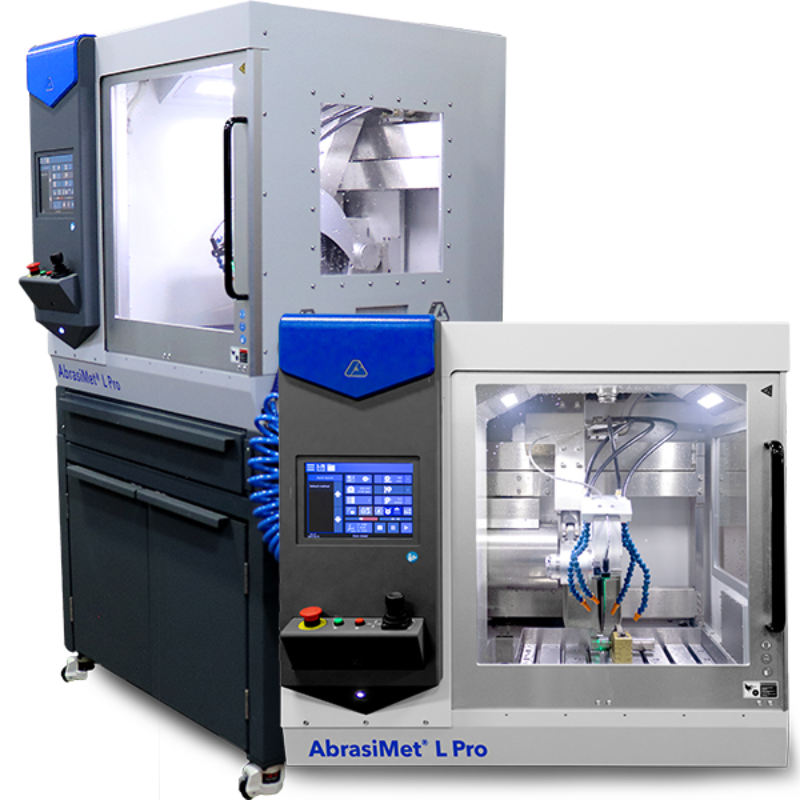
Buehler AbrasiMet XL Pro™ 大型砂轮切割机
AutoMet™ 300 Pro 研磨抛光机
多功能硬度计 UH4000 | 美国威尔逊硬度计 Wilson
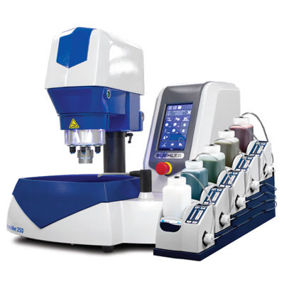
美国标乐 Buehler | AutoMet™ 250 研磨抛光机
美国标乐 Buehler | EcoMet 30 磨抛机
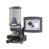
PlanarMet™ 300台式预磨机
MiniMet 1000 半自动磨抛机
美国标乐 Buehler | IsoMet HS 高速精密切割机
美国标乐 Buehler | SimpliMet 4000自动镶嵌机
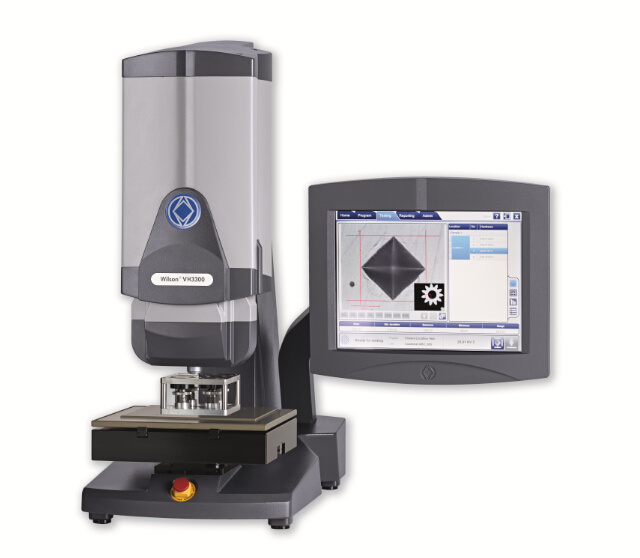
全自动维氏/努氏硬度计 VH3300 | 美国威尔逊硬度计
DiaMet 硬度测试软件
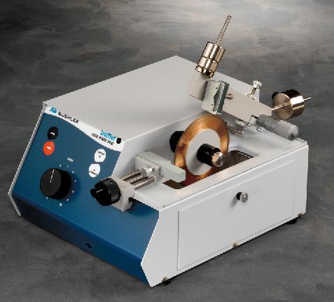
IsoMet 1000精密切割机

关注

拨打电话

留言咨询