| 供货周期: | 一周 |
| 品牌: | 2D SEMICONDUCTOR |
| 货号: | 4601563 |


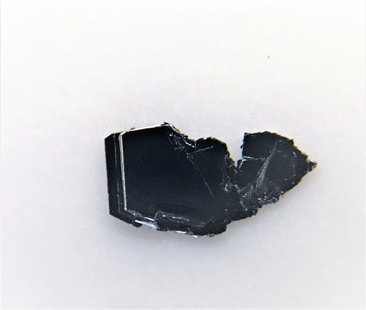
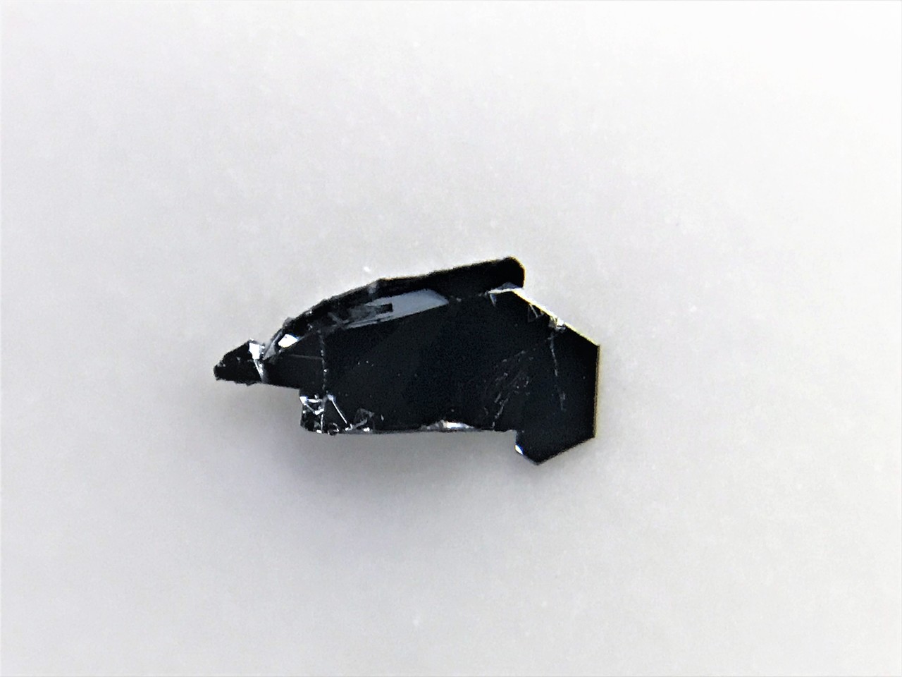
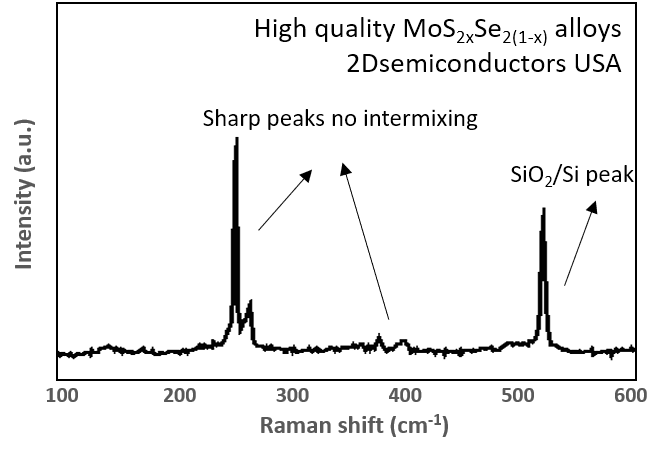
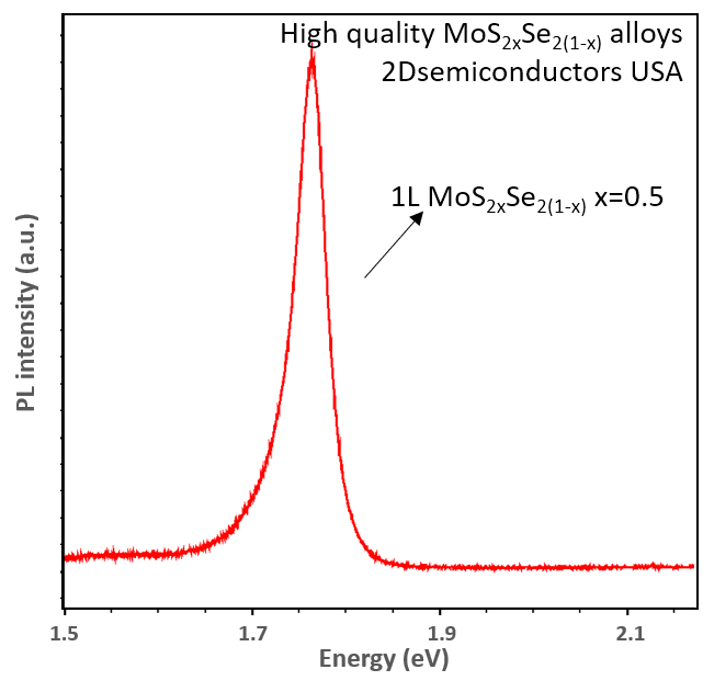
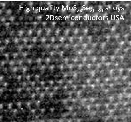
Our MoSSe alloys with the chemical formula MoS2xSe2(1-x) crystals perfectly crystallize in 2H phase and come at different alloy ratios x. Our crystals are grown using two different techniques through chemical vapor transport (CVT) or flux zone growth (see description of these two methods below) and their composition values were determined by XPS, SAED, and EDS measurements.. These crystals all possess extremely narrow PL bandwidths, display clean PL spectra, high carrier mobility, extremely clean and sharp XRD peaks, and negligible amount of defects (see published results as well as CVT vs. Flux based methods below ). These crystals come with guaranteed alloying and valleytronic response, sharp PL, and good electronic response.
Important advantages of our crystals
1. Crystals come fully characterized using macro, micro, and nanoscale measurements (see below)
2. Thanks to our improved flux zone growth method, our crystals are homogeneously alloyed which means across the specimen you will only find one particular x composition.
3. No separation: Phase separation is commonly observed in 2D TMDCs alloys when cooling profiles are not controlled carefully. Our R&D team has worked over five (5) years to solely solve this problem.
Properties of layered MoSSe alloys
Growth method matters> Flux zone or CVT growth method? Contamination of halides and point defects in layered crystals are well known cause for their reduced electronic mobility, reduced anisotropic response, poor e-h recombination, low-PL emission, and lower optical absorption. Flux zone technique is a halide free technique used for synthesizing truly semiconductor grade vdW crystals. This method distinguishes itself from chemical vapor transport (CVT) technique in the following regard: CVT is a quick (~2 weeks) growth method but exhibits poor crystalline quality and the defect concentration reaches to 1E11 to 1E12 cm-2 range. In contrast, flux method takes long (~3 months) growth time, but ensures slow crystallization for perfect atomic structuring, and impurity free crystal growth with defect concentration as low as 1E9 - 1E10 cm-2. During check out just state which type of growth process is preferred. Unless otherwise stated, 2Dsemiconductors ships Flux zone crystals as a default choice.
http://meetings.aps.org/Meeting/MAR18/Session/K36.3
http://meetings.aps.org/Meeting/MAR17/Session/V1.14


相关产品
GO 氧化石墨烯 (Graphene Oxide)
Carboxyl Graphene 羧基石墨烯
Graphene Fluoride 氟化石墨烯
PMMA涂层/预处理石墨烯(进口)
PET基底石墨烯(进口) Graphene on PET
铜基石墨烯薄膜(5*5cm)
铜基石墨烯薄膜(10*10cm)
PET基底石墨烯薄膜(1*1cm)
硅基底石墨烯薄膜(1*1cm)
基于SiO2/Si晶片的双层CVD石墨烯薄膜(4片装)
基于SiO2/Si晶片的双层CVD石墨烯薄膜(8片装)
Monolayer Black Phosphorus Solution 单层黑磷溶液
PtSe2 二硒化铂晶体 (Platinum Diselenide)
白云母(1片装) MICA muscovite V1
白云母(5片装) MICA muscovite V1
详细地址

关注

拨打电话

留言咨询


