产品详情
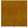
Period: 292nm pitch nominal, one dimensional array. Accuracy is +/- 1%. Calibration certificate will give the actual pitch of the standard.
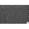
Surface structure: Titanium lines on Silicon, 4x3mm dimensions. Line height (about 30nm) and line width (130nm) are not calibrated.
Usability: The calibrated pattern covers the entire chip. There is sufficient usable area to make tens of thousands of measurementswithout reusing any areas contaminated or altered by previous scans.
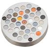
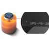
AFM: Use in contact, tapping and other modes with image sizes from 500nm to 20um. Mounted on a 12mm steel AFM disk.
SEM, Auger, FIB: Can be used for a wide range of accelerating voltage (<1kV-30kV) and calibrates images from 5kX to 200kX. Can be supplied unmounted or mounted on an SEM stub of your choice.
Certification: There is a version with a non-traceable manufacturer’s certificate stating average pitch, based on batch measurements.
There is also the traceable, certified version measured in comparison with a standard calibrated at PTB (Physiklisch-Technischen Bundesanstalt in Braunschweig, Germany, is the German counterpart of NIST). The standard is NIST traceable by virtue of the mutual recognition agreement by NIST and PTB.