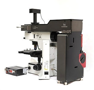

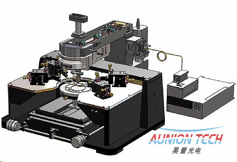
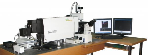
高速大面积共聚焦拉曼成像系统
报价 ¥40万 - 50万

 仪器对比
仪器对比


 关注
关注
 样本下载
样本下载


惊爆价!50万RMB!高速大面积共聚焦拉曼成像系统
高速大面积共聚焦拉曼成像系统,高速Mapping!
XperRam Compact激光拉曼成像系统
超高性价比激光拉曼成像光谱仪
特惠价50万人民币,一套完整的激光拉曼扫描成像系统,同时可用于荧光,光电流成像
高分辨率!
出色的重复性!
使用全息透射光栅,光透过率高!
可扩展/ 定制!
200μm x 200μm 图像快速扫描 & 2D Mapping!
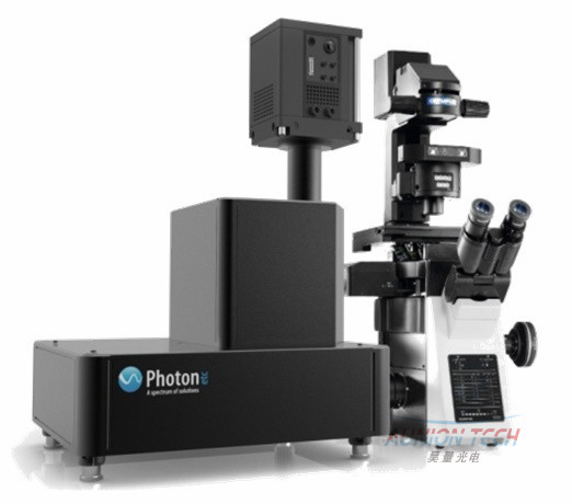
韩国NANOBASE公司专业生产高性价比共聚焦拉曼成像系统,为科学和工业领域提供高性价比解决方案。新用户可以从购买基础款的XperRam Compact型拉曼光谱仪开始,之后可以通过不同的选项对拉曼光谱仪进行升级,以满足用户的不同需求。本产品具有超高性价,目前特惠价50万人民币,包含一套完整的激光拉曼扫描成像系统,同时可用于荧光,光电流成像
共焦拉曼成像系统,共聚焦拉曼成像系统,共焦拉曼光谱成像系统,共焦拉曼成像光谱仪系统,拉曼光谱仪,成像光谱仪,激光拉曼成像系统, 显微拉曼成像系统
韩国NANOBASE公司专业生产共聚焦激光扫描拉曼成像系统,为科学和工业领域提供高性价比解决方案。
产品具有如下特点:
u 独特的激光扫描技术,具有优异的扫描分辨率和重复性
激光扫描分辨率< 0.02 um & 重复性< 0.1 μm
u 体相全息光栅光谱仪
光透过率>90%,比反射式光栅高30%,信号传输效率更高
u 具有Raman/PL/光电流等多种测量模式
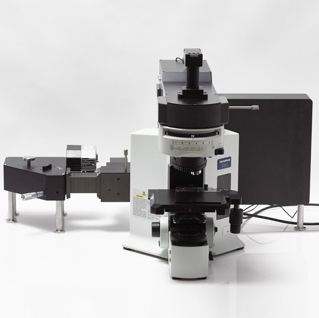
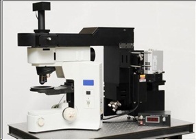
u 结构紧凑,模块化设计
u 扫描速度快,扫描范围大
200μm x 200μm范围内高速成像 & 2D Mapping (x 40 objective)
产品参数:
XperRam Compact | Xpl | |
空间分辨率 | 400nm | 400nm |
最低波数 | 750px-1 | 2500px-1 |
光谱分辨率 | 37.5px-1 | 15px-1 |
光谱范围 | 750px-1到150000px-1 | 2500px-1到87500px-1 |
CCD | ICX674,1392X1452 pixels TE制冷科学级CCD | 1024x256 TE制冷科学级相机 |
激光器 | 532nm,可选配785 | 532nm,可选配785nm
|
Mapping | 拉曼,荧光,光电流 | 拉曼成像需要额外选购 |
物镜 | 10X,40X,100X | 10X,50X,100X |
光栅 | 透射式光栅,效率比反射式高30% | 反射式光栅 |
上表是XperRam Compact与某知名公司拉曼光谱仪参数对比
应用实例:
u 光电流成像,大(重)样品测试
扫描成像,载物台无需移动,故而可以放置很重的样品在载物台上,下图是测量带制冷器的碳纳米管的光电流成像,普通拉曼成像系统无法完成此项测试
u 拉曼成像(二硫化钼) 
图(a)样品台上放置的带制冷器的碳纳米管的显微图像
图(b)碳纳米管的光电流mapping图样,
设置为激光扫描区域180um x180μm,步2μm
可任意设置激光扫描范围和扫描步进,激光扫描范围在40倍物镜下最大可达200μm x 200μm,激光扫描步进可低至0.1μm


图(c)二硫化钼样品的显微图像
图(d)二硫化钼的强度mapping成像,设置为激光扫描区域50um x50μm,激光扫描步进 0.3μm
图(e)二硫化钼的强度mapping成像,设置为激光扫描区域30um x30μm,激光扫描步进 0.1μm
图(f)二硫化钼的频率mapping成像,设置为激光扫描区域30um x30μm,激光扫描步进 0.1μm
图(g)单层与多层二硫化钼薄膜拉曼成像与拉曼峰频移
u 荧光PL成像:
使用Nanobase XperRam系列拉曼成像光谱仪发表的部分文献:
(1) A Van Der Waals Homojunction: Ideal p–n Diode Behavior in MoSe2.pdf- Advanced Materials
(2) SemiconductorInsulator Semiconductor Diode Consisting of Monolayer MoS2, h?BN, and GaN Heterostructure.pdf–ACS Nano
摘要:We propose a semiconductorinsulatorsemiconductor (SIS) heterojunction diode consisting of monolayer (1-L) MoS2, hexagonal boron nitride (h-BN), and epitaxial p-GaN that can be applied to high-performance nanoscale optoelectronics. The layered materials of 1-L MoS2 and h-BN, grown by chemical vapor deposition, were vertically stacked by a wet-transfer method on a p-GaN layer. The final structure was verified by confocal photoluminescence and Raman spectroscopy. Currentvoltage (IV) measurements were conducted to compare the device performance with that of a more classical pn structure. In both structures (the pn and SIS heterojunction diode), clear current-rectifying characteristics were observed. In particular, a current and threshold voltage were obtained for the SIS structure that was higher compared to that of the pn structure. This indicated that tunneling is the predominant carrier transport mechanism. In addition, the photoresponse of the SIS structure induced by the illumination of visible light was observed by photocurrent measurements.
关键词:monolayer MoS2 . h-BN . GaN . semiconductorinsulatorsemiconductor diode . carrier tunneling
摘要:Micro-Raman spectroscopy, X-ray diffraction, high-resolution transmission electron microscopy (TEM), oxygen vacancies, synchrotron X-ray absorption spectroscopy, magnetizations, optical band gaps, and photovoltaic (PV) effects have been studied in (Bi1 – xLax)FeO3 (BFO100xL) ceramics for x = 0.0,0.05, 0.10, and 0.15. XRD, Raman spectra, and TEM confirm a rhombohedral R3c symmetry with the tilted FeO6 oxygen octahedra in all compounds. The low-frequency Raman vibrations become broader and shift toward higher frequency as La3+ increases. Fe K-edge synchrotron X-ray absorptions reveal that Fe3+ valence and Fe–O–Fe bond angle are not modified by the La3+ substitution. All compounds exhibit a linear antiferromagnetic feature. Optical transmission reveals band gaps in the range of 2.22–2.24 eV. The heterostructures of indium tin oxide (ITO) film/(Bi1 – xLax)FeO3 ceramics/Au film show a p–n junction-like I–V characteristic behavior. The maximal PV power conversion efficiency can reach 0.19% in ITO/BFO15L/Au under illumination of k = 405 nm. A junction-like theoretical model can reasonably describe open-circuit voltage and short-circuit current as a function of illumination Intensity
(4) Enhanced photovoltaic effects in A-site samarium doped BiFeO3 ceramics: The roles of domain structure and electronic state .pdf– JECS
摘要:This work reports enhanced photovoltaic (PV) responses of (Bi1 ? xSmx)FeO3 (x = 0.0, 0.05, 0.10) ceramics (BFO100xSm) with ITO film under near-ultraviolet irradiation ([1] = 405 nm). The ceramics were characterized by micro-Raman scattering, high-resolution transmission electron microscopy, and synchrotron X-ray absorption spectroscopy (XAS). A rhombohedral R3c symmetry with tilted FeO6 octahedra has been
confirmed. The Fe K-edge absorption spectra reveal a slight shift toward higher energy as A-site Sm3+ substitution increases. The oxygen K-edge XAS reveals an enhancement of hybridization between the O 2p and unoccupied Fe 3d states due to Sm doping. The optical band gaps are in the range of 2.15–2.24 eV. The maximal PV power-conversion and external quantum efficiencies respectively reach 0.37% and 4.1% in the ITO/BFO5Sm/Au heterostructure. The PV responses can be described quantitatively by a p-n-junctionlike model. The domain structures and hybridization between the O 2p and Fe 3d states play important roles for the PV responses.
摘要:Soft X-ray absorption (XAS), transmission electron spectroscopy (TEM), Raman spectroscopy, and synchrotron XRD have been studied in B-site 0–2 mol% manganese (Mn) doped (Bi0.5Na0.5)0.925Ba0.075TiO3 (BN7.5BT) relaxor ferroelectric ceramics. High-resolution synchrotron XRD and TEM reveal two phase coexistence of rhombohedral R3c and tetragonal P4bm structures in 0 and 0.2%, and an orthorhombic structure in 1 and 2% Mn-doped BN7.5BT at room temperature. Raman spectra of 0% Mn reveal structural transition from two phase coexistence to tetragonal phase near 190 ?C with a softening anomaly, while 0.2–2% Mn-doped BN7.5BT show softening behavior near 290 ?C upon heating. Raman spectra and synchrotron XRD indicate that Mn doping can enhance structural thermal stability in BN7.5BT ceramics.© 2015 Elsevier Ltd. All rights reserved.
关键词:Relaxor ferroelectric ceramics; Raman spectroscopy; Synchrotron XRD; Phase transition
(6)Raman vibrations and photovoltaic conversion in rare earth doped (Bi0.93RE0.07)FeO3 (RE?Dy, Gd, Eu, Sm) ceramics.pdf–CERAMICS INTERNATIONAL
摘要:High-resolution Raman spectra, X-ray diffraction, oxygen vacancies, synchrotron X-ray absorption spectroscopy, magnetization, optical bandgap, and photovoltaic (PV) conversion have been studied in BiFeO3 (BFO) and (Bi0.93RE0.07)FeO3 (RE?Dy, Gd, Eu and Sm) multiferroicceramics (7%Dy–BFO, 7%Gd–BFO, 7%Eu–BFO, and 7%Sm–BFO). 7%Dy–BFO exhibits a weak ferromagnetic behavior instead of the linearantiferromagnetic responses found in the other compounds. Optical transmissions reveal band gaps of 2.20–2.21 eV, which are slightly smallerthan 2.24 eV in pure BFO. The current vs. voltage (I–V) characteristic curves of indium tin oxide (ITO)/(Bi0.93RE0.07)FeO3 ceramics/Auheterostructures suggest a p–n-junction-like behavior. The maximal PV power-conversion efficiencies under illumination of λ?405 nm in ITO/7%Dy–BFO/Au, ITO/7%Gd–BFO/Au, ITO/7%Eu–BFO/Au, and ITO/7%Sm–BFO/Au respectively reach 0.22%, 0.35%, 0.27%, and 0.24%,which are much larger than 0.017% in ITO/BFO/Au. The PV open-circuit voltage and short-circuit current can be reasonably described by ajunction model as a function of illumination intensity.
关键词:Rare-earth doped BiFeO3 ceramics; Raman vibration; Structure; Optical band gap; Photovoltaic conversion
应用领域:
材料学,功能材料,纳米材料,二维材料(石墨烯,二硫化钼等),铁电陶瓷等
生物医学,细胞成像,疾病检测,皮肤分析等
半导体,太阳能电池和OLED等


- 相关仪器
- 相关资料


相关产品

