
| 供货周期: | 一周 |
| 品牌: | 2D SEMICONDUCTOR |
| 货号: | 4601047 |


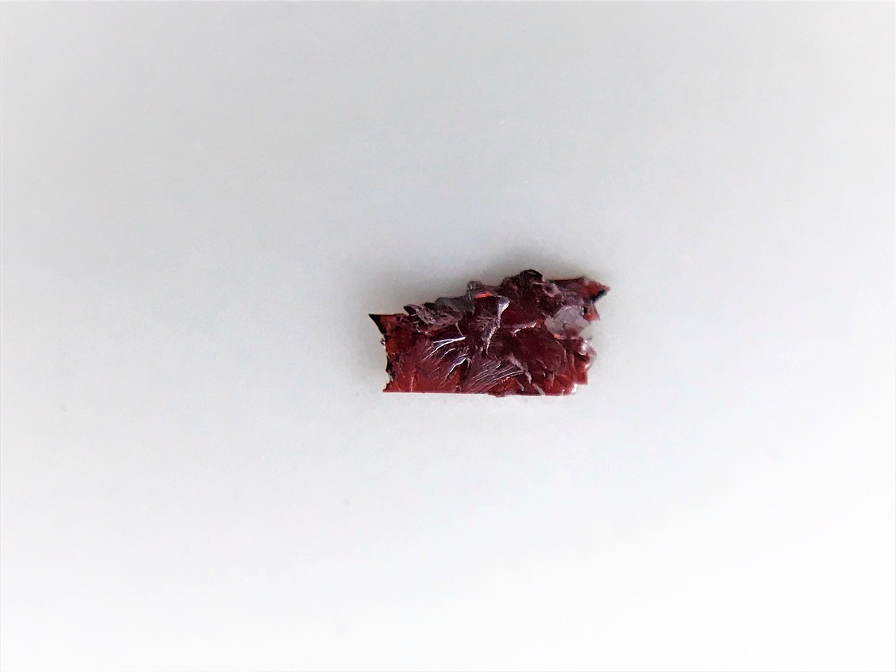
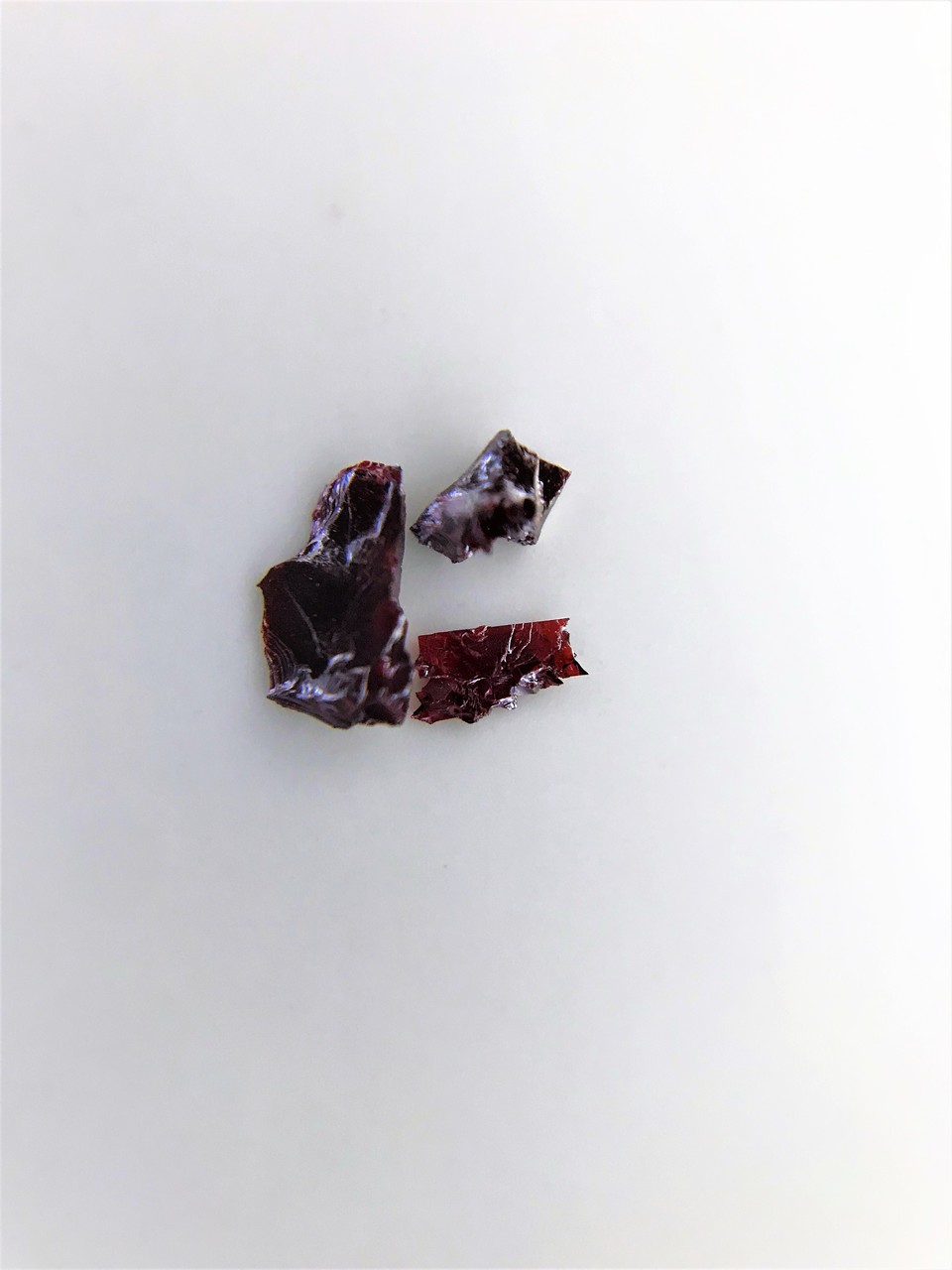
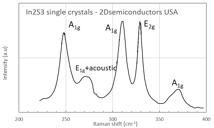
Gamma layered phase of In2S3 is a direct gap semiconductor with an optical band gap ranging from 2 eV - 3.25 eV. It's fundamental band gap nature (direct vs indirect) and its value have been much debaded in the field and remains open ended. In2S3 is particular attractive semiconductor for photoelectrochemical, solar cell, and photonic applications. Typical crystal sizes range in few-mm in size and each order contains 5-7 pieces of In2S3 crystals. The crystals appear layered but is harder to exfoliate compared to molybdenum disulfide. Thus, we recommend using highly adhesive tapes, ultrasonic exfoliation, or other methods to yield atomically thin sheets.
相关产品
GO 氧化石墨烯 (Graphene Oxide)
Carboxyl Graphene 羧基石墨烯
Graphene Fluoride 氟化石墨烯
PMMA涂层/预处理石墨烯(进口)
PET基底石墨烯(进口) Graphene on PET
铜基石墨烯薄膜(5*5cm)
铜基石墨烯薄膜(10*10cm)
PET基底石墨烯薄膜(1*1cm)
硅基底石墨烯薄膜(1*1cm)
基于SiO2/Si晶片的双层CVD石墨烯薄膜(4片装)
基于SiO2/Si晶片的双层CVD石墨烯薄膜(8片装)
Monolayer Black Phosphorus Solution 单层黑磷溶液
PtSe2 二硒化铂晶体 (Platinum Diselenide)
白云母(1片装) MICA muscovite V1
白云母(5片装) MICA muscovite V1

关注

拨打电话

留言咨询


