| 供货周期: | 一周 |
| 品牌: | 2D SEMICONDUCTOR |
| 货号: | 4602753 |


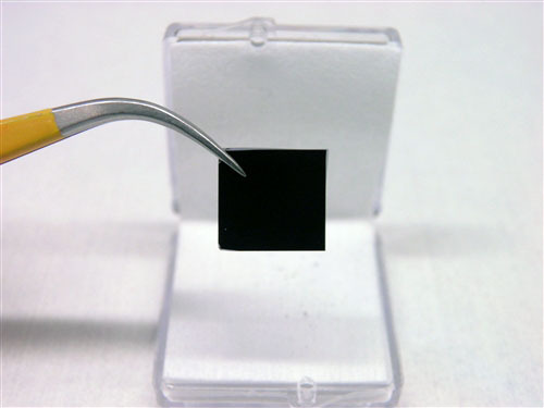
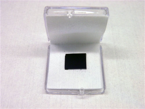
Monolayer tungsten diselenide (1H-WSe?) flakes have been exfoliated from bulk tungsten diselenide (2H-WSe?) onto 90nm thermal oxide and measures from 5micron up to 40micron in size. Each sample contains at least one single-layer WSe? and is easy to find with the given x and y coordinates. Full characterization is performed on each monolayer flake. Typically, single-layer WSe? show strong PL at 1.66eV with 0.04 to 0.08eV FWHM, and the Raman peaks are located at 139.5cm-1 (E2g in-plane mode) and 249.5 cm-1 (A1g out-of-plane mode). All the data is provided with the sample and data includes Raman, photoluminescence, 100x optical images, and x,y coordinates.
Characterization
Raman spectroscopy: Raman spectroscopy is data is taken on every single-layer flakes. Typically, flakes show two prominent Raman peaks at 139.5cm-1 (E2g- in plane-) and 249.5cm-1 (A1g out-of-plane) and the FWHM (full-width-at-half-maximum) is less than 5cm-1. Photoluminescence (PL): In the single layer form, tungsten diselenide possesses direct band-gap at 1.65eV. PL measurements show strong PL peak located at 1.66eV with 0.04-0.08 eV PL FWHM.
Optical Microscope images: Each sample is inspected under the optical microscope and x-y coordinates are recorded.
Contact us for more information
Possible applications:
Electronics
Sensors - detectors
Optics
STM - AFM applications
Molecular detection - binding
Ultra-low friction studies
Materials science and semiconductor research

相关产品
GO 氧化石墨烯 (Graphene Oxide)
Carboxyl Graphene 羧基石墨烯
Graphene Fluoride 氟化石墨烯
PMMA涂层/预处理石墨烯(进口)
PET基底石墨烯(进口) Graphene on PET
铜基石墨烯薄膜(5*5cm)
铜基石墨烯薄膜(10*10cm)
PET基底石墨烯薄膜(1*1cm)
硅基底石墨烯薄膜(1*1cm)
基于SiO2/Si晶片的双层CVD石墨烯薄膜(4片装)
基于SiO2/Si晶片的双层CVD石墨烯薄膜(8片装)
Monolayer Black Phosphorus Solution 单层黑磷溶液
PtSe2 二硒化铂晶体 (Platinum Diselenide)
白云母(1片装) MICA muscovite V1
白云母(5片装) MICA muscovite V1

关注

拨打电话

留言咨询


