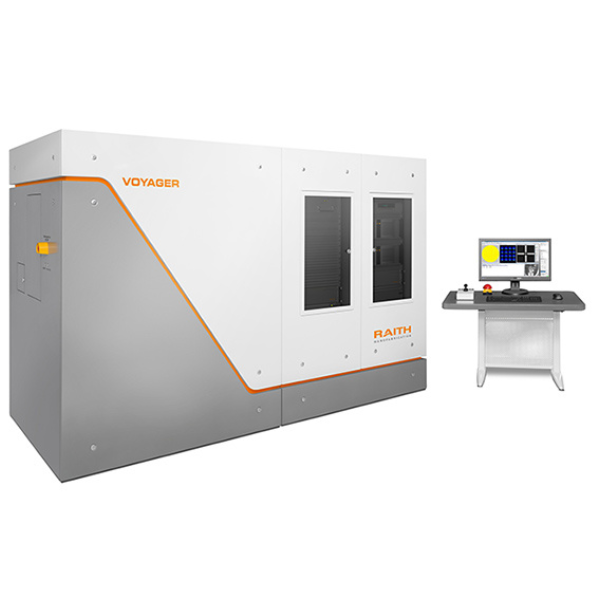
| 型号: | VOYAGER 2 |
| 产地: | 德国 |
| 品牌: | Raith |
| 评分: |
|


Raith 电子束光刻机
1.系统适用于2"及以下的样片,采用热场发射电子枪,加速电压为20V~30kV。可实现高分辨电子束曝光,最小验收线宽≤8nm。
2.系统中集成了高精度的激光干涉工作台,运动行程为50 x 50 x 25mm,XY方向定位精度2nm,可以实现精确的拼接套刻,拼接套刻精度≤50nm。
3.系统兼具了高精度成像度量的功能,其成像效果和市面上中高端的热场电镜类似,放大倍数为20x ~1,000,000x。
4.另外,除了标准配置, 客户还可以增加一些选配件,如选配背散射探测器、能谱仪等,进行材料分析;选配工作台旋转倾斜模块,实现不同角度的材料成像等。如果选择相应的选配件,请增加相应的价格。
3D SEM image mosaics stitched over large areas and in 3D with CAD shape extraction
The CHIPSCANNER combines high-resolution electron optics, multiple high-efficiency electron detectors, and ultra-precise Laser Interferometer Stage technology with unique software to deliver homogenous large-area image mosaics for each layer with minimum stitching errors and stable brightness/contrast values and CAD shape extraction. With features such as
• Active focus control using laser height sensing
• Highest position and beam accuracy and stability, and
• A wide range of selectable electron detectors,
the CHIPSCANNER produces the most accurate large-area, high-resolution image mosaics directly acquired by an SEM instrument. Since the absolute position of each pixel, even over cm², is ultimately known to the accuracy provided by the laser interferometer stage and ultra-precise image calibrations, these images can be precisely stacked (3D-stitched).
Various high-speed detectors, flexible working distance, parallel detector stream handling and a high-speed scan generator allow precise and flexible image acquisition that is also high throughput.
Large-area, ultra-high-resolution 3D SEM imaging applications in chip reverse engineering, materials science, and life sciences (e.g. connectomics) require surfaces of up to cm² areas to be scanned with nm resolution and excellent layer to layer accuracy (‘3D stitching’) for layout and schematic extraction or 3D modeling. While traditional SEM instruments are inherently limited by small, uncalibrated fields of view (FOVs) and imprecise sample positioning, the CHIPSCANNER addresses these challenges by combining the resolution and flexibility of an SEM instrument with the accuracy, stability, and automation of an electron beam lithography (EBL) instrument – a core area of expertise at Raith. High-resolution, large-area image mosaics are created by capturing sequential SEM images and stitching them together for further analysis, while the laser interferometer stage and field-of-view calibration reduce overlap to an absolute minimum and thus reduce required computing. A true large-area 3D SEM!
相关产品
高温熔炼和晶体生长电弧炉 法国ECM
激光加热基座晶体生长炉 法国Cyberstar
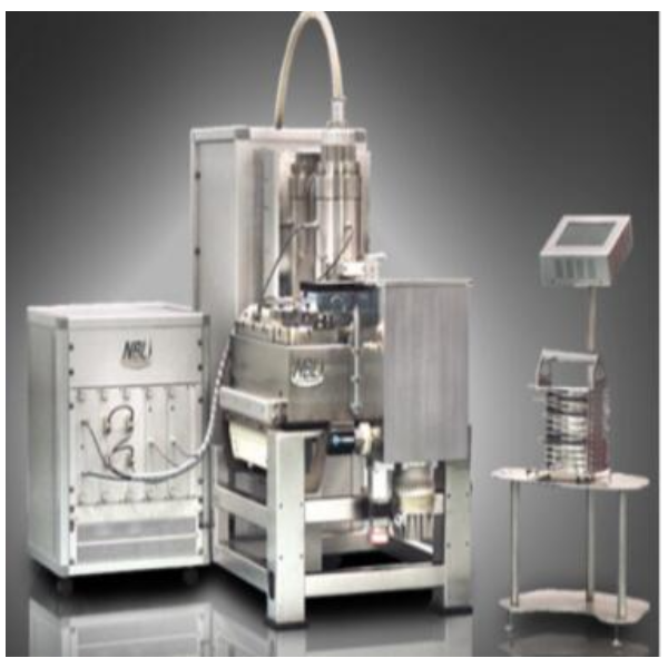
英国Nanobean NB5 电子束光刻机
K1-Fluo DMB科研级倒置共聚焦显微镜 Nanoscope system
NS200便携式激光拉曼光谱系统 Nanoscope system
NS3500三维激光共聚焦显微镜Nanoscope system
PVD&ALD集群系统
Swiss Cluster ALD高性能原子层沉积系统3D材料
Swiss Cluster ALD原位多层复合原子层沉积系统
12寸磁控溅射、电子束蒸发 英国Korvus 手套箱集成
PVD集群系统-多腔体 英国Korvus
桌面式磁控溅射仪 英国Korvus(兼容手套箱)
桌面式电子束蒸发E-beam 英国Korvus
LEED低能电子衍射仪 美国LK
俄歇电子能谱仪 美国LK

关注

拨打电话

留言咨询