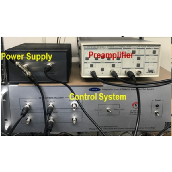
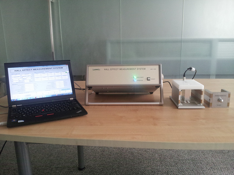
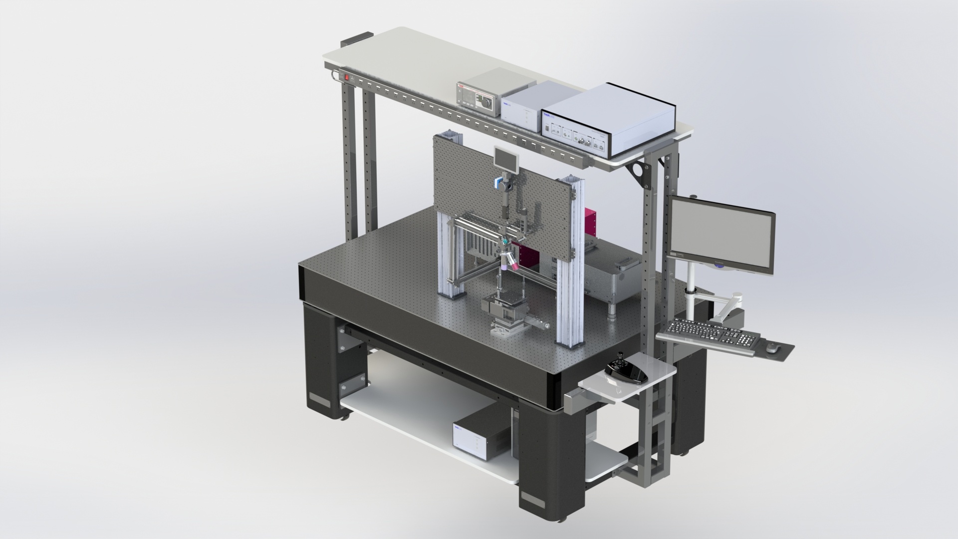
We offer custom SEE laser testing solutions:Single photonTwo photonsSelection of Pico and Femto second lasersShortwave 900nm to 1700nm and Visible imaging systemMicroscope objective choices 200X, 100X, 50X 20XAdditional Features:High accuracy X-Y-Z motorized stages ( nm resolution) 50mm travel XYZ, 0.1micron resolution Joystick for X-YTilt stat ( 3 rotation axes) manual micrometer or motorizedProtective enclosureDual microscope objective top and bottom (optional)Replace Synchrotron beam-line time and high costFor space, military, aerospace, Railways, Automotive, AvionicApplications:SEU: Single Event UpsetSET: Single Event TransientSEL: Single Event Latch-upSEGR: Single Event Gate RuptureSEB: Single Event BurnoutSEGR: Single Event Gate RuptureSEFI: Single Event Functional InterruptSingle‐Event Effect (SEE): Any measurable or observable change in state or performance of a microelectronic device, component, subsystem, or system (digital or analog) resulting from a single energetic particle strike.Single‐Event Transient (SET): A soft error caused by the transient signal induced by a single energetic particle strike.Single‐Event Latch‐up (SEL): An abnormal high‐current state in a device caused by the passage of a single energetic particle through sensitive regions of the device structure and resulting in the loss of device functionality. SEL may cause permanent damage to the device. If the device is not permanently damaged, power cycling of the device (off and back on) is necessary to restore normal operation. An example of SEL in a CMOS device is when the passage of a single particle induces the creation of parasitic bipolar (p‐n‐p‐n) shorting of power to ground. Single‐Event Latch‐up (SEL) cross‐section: the number of events per unit fluence. For chip SEL cross‐section, the dimensions are cm2 per chip. If the charge generated by a single high LET particle is collected by a single high LET particle is collected by a sensitive node of the device or circuit, and this charge is larger than the critical charge required to start an anomalous behaviour an effect singe even effect, may be seen affecting the electrical performance of the device or circuit such as soft errors or hard destructive errors. Space systems often require electronics that can operate in a high-radiation environment. This radiation may result from particles trapped in planetary magnetic fields (e.g., the Van Allen belts which affect Earth-orbiting satellites or the intense radiation fields of Jupiter and its moons), galactic cosmic rays, or high-energy protons from solar events. At low Earth orbit, an integrated circuit may be exposed to a few kilorads of radiation over its useful lifetime, while at orbits in the middle of the Van Allen belts, exposure levels may increase to several hundred kilorads or more. In addition to the natural space environment, military satellites must be able to survive transient bursts of radiation resulting from a hostile nuclear explosion. To achieve these higher levels, radiation-hardened integrated circuits are required. In general, these circuits are fabricated using specialized processes and designs that increase their tolerance to ionizing radiation by several orders of magnitude. Semiconductor FailuresThe primary effects of natural space radiation on spacecraft electronics are total ionizing dose (TID) and single event effects (SEE). TID creates bulk-oxide and an interface-trap charge that reduces transistor gain and shifts the operating properties (e.g., threshold voltage) of semiconductor devices. TID accumulation will cause a device to fail if (1) the transistor threshold voltage shifts far enough to cause a circuit malfunction, (2) the device fails to operate at the required frequency, and/or (3) electrical isolation between devices is lost. SEE occurs when a cosmic ray or other very high-energy particle impinges on a device. The particle generates a dense track of electron-hole pairs as it passes through the semiconductor, and those free carriers are collected at doping junctions. The net effect is that the circuit is perturbed and may lose data (called a single-event upset or SEU). The passage of a sufficiently energetic particle through a critical device region can even lead to permanent failure of an IC due to single-particle-event latchup (SEL), burnout, or dielectric/gate rupture. In general, components that exhibit SEL are not acceptable for space applications unless the latchup can be detected and mitigated. Burnout and gate rupture are especially problematic for high-voltage and/or high-current electronics associated with space-borne power supplies. SEE have become an increasing concern as ICs begin to use smaller device geometries and lower operating voltages, leading to reduced nodal capacitance and charge stored on circuit nodes. In addition to these primary effects, displacement damage effects caused by high-energy protons and electrons can reduce mission lifetimes due to long-term damage to CCDs, optoelectronics, and solar cells.Radiation ProtectionRadiation-hardened technology is often characterized as technology in which the manufacturer has taken specific steps (i.e., controls) in materials, process, and design to improve the radiation hardness of a commercial technology. Consider the case of CMOS technology, whose low power and voltage requirements make it a popular candidate for space applications. The most likely failure mechanism for CMOS devices resulting from TID is a loss of isolation caused by parasitic leakage paths between the source and drain of the device. For improved TID hardness, changes in the isolation structure may be required, e.g., a heavily-doped region or "guardband" can be formed by ion implantation that effectively shuts off radiation-induced parasitic leakage paths. In addition, a low thermal budget and minimum hydrogen during processing has been found to improve TID hardness. The use of oversized transistors and feedback resistors, capacitors, or transistors can be implemented for improved SEE immunity. For improved latchup and transient immunity, the change can sometimes be as simple as use of a thin epitaxial substrate. SOI technology that employs an active device layer built on an insulating substrate can (with proper design) provide significant improvement in SEE and transient tolerance. There are also several design approaches that can be used to increase radiation hardness. One global design change is the conversion of dynamic circuitry to full static operation, thereby placing data in a more stable configuration that is less susceptible to the perturbing effects of radiation. For TID, n-channel transistors can be designed in "closed" geometry that shuts off parasitic leakage paths. For SEU, memory cells with additional transistors can provide redundancy and error-correction coding (ECC) to identify and correct errors. Design approaches for improved radiation hardness generally result in a performance and layout area penalty. Unless specific steps such as these are taken during the design and manufacture of a device, radiation hardness levels are typically low and variable.Non-Hardened TooUnhardened, commercial CMOS circuits are typically able to withstand TID levels in the range from 5 to 30 kilorads at space-like dose rates. (The commonly used unit of TID is the rad, i.e.,radiation absorbed dose. One rad is equal to an adsorbed energy of 100 ergs per gram of material.) However, there are many space missions in which commercial CMOS technology may be used. In these missions (e.g., low Earth orbit), the spacecraft may be exposed to only a few kilorads of TID during its lifetime. As an example, Space Station Freedom may require integrated circuits with hardening requirements ranging from a few to 20 kilorads depending on platform location. In these applications, shielding and careful screening of technology (to take advantage of annealing in the space environment) enables the use of some unhardened, commercial technology. Historically, bipolar circuits have been very tolerant to total ionizing dose. Recently, major advances in bipolar technology have been due, in part, to the introduction of "recessed oxides." The recessed oxide lateral dielectric isolation acts as a diffusion stop, and minimizes junction capacitances. Thus, recessed oxides allow much smaller feature size, increased packing density, and higher speed. However, when irradiated, several parasitic leakage paths can be formed including buried layer to buried layer channeling, collector to emitter channeling on wallin: 0px "Single photonTwo-photonScreening devices with different designs in the same technology node for SEU-MBU+++(+)Accurate SEU cross section vs LET measurement for a memory device+++++Obtain 3D view of charge collection volumes++
 留言咨询
留言咨询
 400-860-5168转2623


 我要推广仪器
 下载APP
下载APP