面向半导体市场,日立推出3D SEM CT1000和高速缺陷检测SEM CR7300
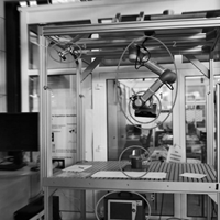
p style="text-align: justify text-indent: 2em "2020年11月,日立宣布推出3D SEM CT1000和高速缺陷检测SEM CR7300。/pp style="text-align: justify text-indent: 2em "3D SEM CT1000是一款主要用于半导体行业缺陷观察的产品。可对直径达8英寸(200 mm)的晶圆在制造过程中出现的图案和缺陷形状进行3D观察,并可分析所观察物体的元素组成。该产品将有助于物联网和车载汽车半导体设备的质量保证。/pp style="text-align: justify text-indent: 2em "高速缺陷检测SEM CR7300是一种新型的扫描电镜,有助于提高尖端半导体器件的生产效率。增强的电子光学可以获得迄今为止最好的高分辨率图像,而先进的成像和控制系统使高速图像采集比传统方法节省一半的时间,大大减少了总检测时间。/pp style="text-align: center "span style="color: rgb(0, 176, 240) "strongspan style="font-size: 18px "【3D SEM CT1000】/span/strong/span/pp style="text-align: center "img style="max-width:100% max-height:100% " src="https://img1.17img.cn/17img/images/202012/uepic/fda3ac17-4b47-4c25-8f8e-9bd15ac248ff.jpg" title="图片1.png" alt="图片1.png"//pp style="text-align: center "strongCT1000相关参数/strong/ptable border="1" cellspacing="0" style="border: none"tbodytr class="firstRow"td width="206" valign="center" style="border: 1px solid rgb(0, 0, 0) padding: 5px "p style=" text-indent: 0 line-height: 19px"span style="font-family: Arial color: rgb(51, 51, 51) letter-spacing: 0 font-size: 13px"Model/span/p/tdtd width="362" valign="center" style="border: 1px solid rgb(0, 0, 0) padding: 5px "p style=" text-indent: 0 line-height: 19px"span style="font-family: Arial color: rgb(51, 51, 51) letter-spacing: 0 font-size: 13px"CT1000/span/p/td/trtrtd width="206" valign="center" style="border: 1px solid rgb(0, 0, 0) padding: 5px "p style=" text-indent: 0 line-height: 19px"span style="font-family: Arial color: rgb(51, 51, 51) letter-spacing: 0 font-size: 13px"Resolution/span/p/tdtd width="362" valign="center" style="border: 1px solid rgb(0, 0, 0) padding: 5px "p style=" text-indent: 0 line-height: 19px"span style="font-family: Arial color: rgb(51, 51, 51) letter-spacing: 0 font-size: 13px"7nm@1kV/span/p/td/trtrtd width="206" valign="center" style="border: 1px solid rgb(0, 0, 0) padding: 5px "p style=" text-indent: 0 line-height: 19px"span style="font-family: Arial color: rgb(51, 51, 51) letter-spacing: 0 font-size: 13px"Maximum sample tilt angle/span/p/tdtd width="362" valign="center" style="border: 1px solid rgb(0, 0, 0) padding: 5px "p style=" text-indent: 0 line-height: 19px"span style="font-family: Arial color: rgb(51, 51, 51) letter-spacing: 0 font-size: 13px"55/spanspan style="font-family: 宋体 color: rgb(51, 51, 51) letter-spacing: 0 font-size: 13px"° /span/p/td/trtrtd width="206" valign="center" style="border: 1px solid rgb(0, 0, 0) padding: 5px "p style=" text-indent: 0 line-height: 19px"span style="font-family: Arial color: rgb(51, 51, 51) letter-spacing: 0 font-size: 13px"Size of observation field/span/p/tdtd width="362" valign="center" style="border: 1px solid rgb(0, 0, 0) padding: 5px "p style=" text-indent: 0 line-height: 19px"span style="font-family: Arial color: rgb(51, 51, 51) letter-spacing: 0 font-size: 13px"0.675 to 135 µ m/span/p/td/trtrtd width="206" valign="center" style="border: 1px solid rgb(0, 0, 0) padding: 5px "p style=" text-indent: 0 line-height: 19px"span style="font-family: Arial color: rgb(51, 51, 51) letter-spacing: 0 font-size: 13px"Elemental analysis (optional)/span/p/tdtd width="362" valign="center" style="border: 1px solid rgb(0, 0, 0) padding: 5px "p style=" text-indent: 0 line-height: 19px"span style="font-family: Arial color: rgb(51, 51, 51) letter-spacing: 0 font-size: 13px"Energy-dispersive X-ray spectrometer/span/p/td/trtrtd width="206" valign="center" style="border: 1px solid rgb(0, 0, 0) padding: 5px "p style=" text-indent: 0 line-height: 19px"span style="font-family: Arial color: rgb(51, 51, 51) letter-spacing: 0 font-size: 13px"Measurable wafer size/span/p/tdtd width="362" valign="center" style="border: 1px solid rgb(0, 0, 0) padding: 5px "p style=" text-indent: 0 line-height: 19px"span style="font-family: Arial color: rgb(51, 51, 51) letter-spacing: 0 font-size: 13px"SEMI standard 200-mm Si wafer/span/p/td/tr/tbody/tablep style="text-align: justify text-indent: 2em "CT1000可自动输送直径达8英寸(200mm)的晶圆,并精确移动到观察缺陷的模块位置。样品台可以倾斜进行3D SEM观察。如果发现缺陷,它可以对相关缺陷进行元素分析。元素分析可以用来分析导致成品率下降的因素,有助于提高半导体器件在开发和制造过程中的质量。在检查完缺陷和图案形状后,晶圆可以返回生产线,提高制造工艺效率。/pp style="text-align: justify text-indent: 2em "CT1000的一个特点是能够使用样品台倾斜功能观察3D SEM图像。为了实现这一功能,日立高新开发了一种锥形物镜,可以使晶圆倾斜55° 。五轴样品台的设计是为了防止晶圆片的中心在从正上方观察时发生明显的移动,即使样品台倾斜到最大的倾角。这样可以更好地捕捉目标缺陷,提高工作效率。/pp style="text-align: center "strongspan style="color: rgb(0, 176, 240) font-size: 18px "【高速缺陷检测 SEM CR7300】/span/strong/pp style="text-align: center "strongspan style="color: rgb(0, 176, 240) font-size: 18px "img style="max-width:100% max-height:100% " src="https://img1.17img.cn/17img/images/202012/uepic/4cee5018-31e6-45b8-83f6-35b1d00e7acc.jpg" title="图片2.png" alt="图片2.png"//span/strong/ppstrongspan style="color: rgb(0, 176, 240) font-size: 18px "/span/strong/pp style="text-align: center "strongCR7300相关参数/strong/ppstrongspan style="color: rgb(0, 176, 240) font-size: 18px "/span/strong/ptable border="1" cellspacing="0" style="border: none"tbodytr class="firstRow"td width="136" valign="center" style="border: 1px solid rgb(0, 0, 0) padding: 5px "p style=" text-indent: 0 line-height: 19px"span style="font-family: Arial color: rgb(51, 51, 51) letter-spacing: 0 font-size: 13px"Model/span/p/tdtd width="433" valign="center" style="border: 1px solid rgb(0, 0, 0) padding: 5px "p style=" text-indent: 0 line-height: 19px"span style="font-family: Arial color: rgb(51, 51, 51) letter-spacing: 0 font-size: 13px"CR7300/span/p/td/trtrtd width="136" valign="center" style="border: 1px solid rgb(0, 0, 0) padding: 5px "p style=" text-indent: 0 line-height: 19px"span style="font-family: Arial color: rgb(51, 51, 51) letter-spacing: 0 font-size: 13px"Wafer Size/span/p/tdtd width="433" valign="center" style="border: 1px solid rgb(0, 0, 0) padding: 5px "p style=" text-indent: 0 line-height: 19px"span style="font-family: Arial color: rgb(51, 51, 51) letter-spacing: 0 font-size: 13px"ø 300 mm (SEMI standard V-notched wafer)/span/p/td/trtrtd width="136" valign="center" style="border: 1px solid rgb(0, 0, 0) padding: 5px "p style=" text-indent: 0 line-height: 19px"span style="font-family: Arial color: rgb(51, 51, 51) letter-spacing: 0 font-size: 13px"Auto-loader/span/p/tdtd width="433" valign="center" style="border: 1px solid rgb(0, 0, 0) padding: 5px "p style=" text-indent: 0 line-height: 19px"span style="font-family: Arial color: rgb(51, 51, 51) letter-spacing: 0 font-size: 13px"Random access compatible with 2FOUP/spanspan style="font-family: Arial color: rgb(51, 51, 51) letter-spacing: 0 font-size: 12px"*5/span/p/td/trtrtd width="136" valign="center" style="border: 1px solid rgb(0, 0, 0) padding: 5px "p style=" text-indent: 0 line-height: 19px"span style="font-family: Arial color: rgb(51, 51, 51) letter-spacing: 0 font-size: 13px"Power Supply/span/p/tdtd width="433" valign="center" style="border: 1px solid rgb(0, 0, 0) padding: 5px "p style=" text-indent: 0 line-height: 19px"span style="font-family: Arial color: rgb(51, 51, 51) letter-spacing: 0 font-size: 13px"Single-phase 200 VAC, 208 V, 12 kVA (50/60 Hz)/span/p/td/tr/tbody/tablep style="text-align: justify text-indent: 2em "strongCR7300具有以下特点:/strong/pp style="text-align: justify text-indent: 2em "1. 通过高吞吐量提高生产率/pp style="text-align: justify text-indent: 2em "新开发的电子光学系统和高速成像系统使快速光束扫描速度达到传统方法的两倍,而加强的晶圆传输系统减少了晶圆装载时间。因此,每小时缺陷成像的总性能大约是以前的工具模型的两倍。自动缺陷检测(ADR)性能与加强的成像技术能够有助于提高先进半导体器件的生产效率。新的EDS(元素分析)系统采用高灵敏度x射线探测器,使缺陷的元素分析时间比以往更快。/pp style="text-align: justify text-indent: 2em "2. 在制造过程中可视化设备的电气特性/pp style="text-align: justify text-indent: 2em "新开发的VT-Scan能够可视化存储设备的电气特性,并在早期制造过程中检测到电气缺陷。/pp style="text-align: justify text-indent: 2em "3. 改善微观缺陷的可见性/pp style="text-align: justify text-indent: 2em "新的电子光学技术使显微缺陷的高分辨率成像成为可能,并利用人工智能(AI)提供先进的图像处理,以进一步提高图像质量。此外,它还具有新开发的暗场光学显微镜无图案晶圆审查功能。可以提高先进工艺开发所需的无图案晶圆上微观缺陷的捕获率。/ppstrongspan style="color: rgb(0, 176, 240) font-size: 18px "/span/strongbr//ppbr//p


 我要推广仪器
 下载APP
下载APP