当前位置: 仪器信息网 > 行业主题 > >

碲化锑

仪器信息网碲化锑专题为您提供2024年最新碲化锑价格报价、厂家品牌的相关信息, 包括碲化锑参数、型号等,不管是国产,还是进口品牌的碲化锑您都可以在这里找到。 除此之外,仪器信息网还免费为您整合碲化锑相关的耗材配件、试剂标物,还有碲化锑相关的最新资讯、资料,以及碲化锑相关的解决方案。

碲化锑相关的耗材

  • 二碲化钛(TiTe2)
    1、企业介绍泰州巨纳新能源有限公司:巨纳集团(Sunano Group)是能源行业的知名品牌。泰州巨纳新能源有限公司(Sunano Energy)是国内最早的从事石墨烯制备、性能检测及应用产品开发的公司之一,注册资本11000万元,有办公用房300多平方米,厂房和洁净室3000多平方米。核心研发团队主要由国内外知名高校博士组成,部分成员来自于2010年诺贝尔物理学奖小组,项目技术处于国际领先地位,在石墨烯领域拥有专利30余项。企业管理团队有丰富的成功创业经验,创新意识强,公司客户遍布全球。2、高质量二维晶体材料简介:二维晶体材料指的是以石墨烯为代表的单原子层及少数原子层厚度的晶体材料。巨纳集团除了提供石墨烯材料、设备、检测等一体化服务外,还联合荷兰HQ Graphene为全球客户提供高质量的类石墨烯二维晶体材料,并提供定制服务,以满足客户的不同需求。 名称:二碲化钛(TiTe2)纯度:>99.995%尺寸:~5mm属性:半导体
  • 碲化锌晶体ZnTe
    [110]晶向的ZnTe碲化锌晶体常通过光学整流来产生太赫兹振荡。光学整流效应是一种二阶非线性效应,也是一种特殊的差频效应。一定宽度的飞秒激光脉冲,拥有非常宽的频率分量,这些分量间的相互作用(主要是差频)将会产生从0到几个太赫兹的电磁波。 太赫兹脉冲可通过另一个自由空间的晶向ZnTe实现光电探测。太赫兹光脉冲会使碲化锌晶体ZnTe产生双折射,因此当太赫兹光脉冲和可见光脉冲同时在(ZnTe)碲化锌晶体中直线传播时,可见光的偏振状态将会因此发生变化。使用λ/4波片,偏振分光体,以及平衡光电二极管,我们可以完成对可见光的偏振状态的监控,从而得知太赫兹光脉冲的振幅,延迟等各种参数。而这种监测太赫兹光脉冲的完整电磁场信息(振幅和相位延迟)的能力,是时域太赫兹光谱仪比较具有吸引力的特性之一。产品简介碲化锌晶体(ZnTe)是一种具有立方闪锌矿结构的电光晶体,通常被应用于THz波的产生以及探测。产品特点: — 应用于THz产生、探测和光学限幅器— 晶体纯度高 99.995%-99.999%— 表面质量优不同厚度碲化锌晶体ZnTe的TDS测试数据:产生端ZnTe晶体厚度为0.5mm,探测端晶体厚度分别为0.5mm,1mm,2mm碲化锌晶体参数规格:晶格结构:立方闪锌矿密度: 5.633 g/ cm3比热:0.16 J/gK带隙 (300 K):2.25 eV最大透过率 (λ =7-12 μm):60 % 最大电阻率:109 Ohm*cm折射率 (λ =10.6 μm):2.7电光系数 r41 (λ =10.6 μm):4.0×10⁻¹² m/V电阻率:a). low: 103 Ohm*cm b). high: 109 Ohm*cm最大 IR-optic blank 直径/长度: 38×20 mm最大单晶尺寸 直径/长度: 38×20 mm碲化锌晶体ZnTe产品:碲化锌晶体ZnTe棒、碲化锌晶体晶圆片、碲化锌晶体窗片和基底直径/边长:1-50 mm厚度/长度:0.1-150 mm晶向:(110), (100), (111)表面质量:As-cut, 80/50, 60/40 per MIL-0-13830
  • 二碲化钛晶体(99.995%) TiTe2(Titanium Ditelluride)
    二碲化钛晶体 TiTe2(Titanium Ditelluride)晶体尺寸:~8毫米电学性能:半金属晶体结构:六边形晶胞参数:a = b = 0.377 nm, c = 0.649 nm, α = β = 90°, γ = 120°晶体类型:合成晶体纯度:>99.995% X-ray diffraction on a TiTe2 single crystal aligned along the (001) plane. XRD was performed at room temperature using a D8 Venture Bruker. The 4 XRD peaks correspond, from left to right, to (00l) with l = 2, 3, 4, 5 Powder X-ray diffraction (XRD) of a single crystal TiTe2. X-ray diffraction was performed at room temperature using a D8 Venture Bruker.Stoichiometric analysis of a single crystal TiTe2 by Energy-dispersive X-ray spectroscopy (EDX).Raman spectrum of a single crystal TiTe2. Measurement was performed with a 785 nm Raman system at room temperature.
  • 碲化锌晶体 ZnTe
    THz晶体The application fields of zinc telluride are THz detectors THz emitters IR optics substrates crystal pieces for vapour deposition optical limiters.Basic propertiesZnTe TransmissionProductsZnTe rods, wafers, windows and substratesZnTe crystal pieces for vapour depositionZnTe/ZnS/ZnSe/CdxZn1-xTe/CdS/CdSe/CdTe/CdSSe/ZnCdS第二和第六周期元素形成的化合物ZnSe, ZnS, ZnTe, CdSe, CdS, CdTe, CdZnTe , CdSSe等均为宽带半导体。其中ZnTe,ZnS可利用全固态可调谐双波长光源在非线性晶体中二阶光学混频方法产生太赫兹光。CdxZn1-xTe(CZT/碲锌镉)半导体单晶是发展远红外,可见光,X-射线探测器,γ射线探测器的重要材料。CZT射线探测器具有吸收系数大,结构紧凑,室温操作等优点。而现在工业和医疗方面产用的高纯Ge和Si的探测器,只能工作在液氮温度下。CZT已经成为硬X射线和γ射线的一种关键技术。天文学方面用CZT阵列去研究宇宙中的高能γ射线源
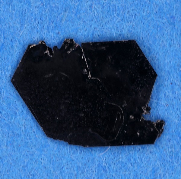
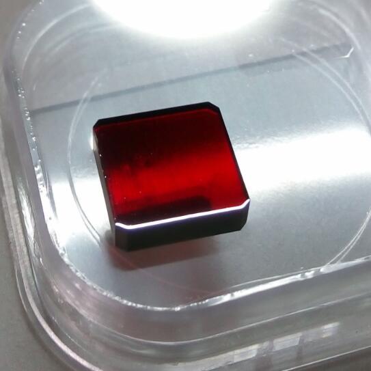
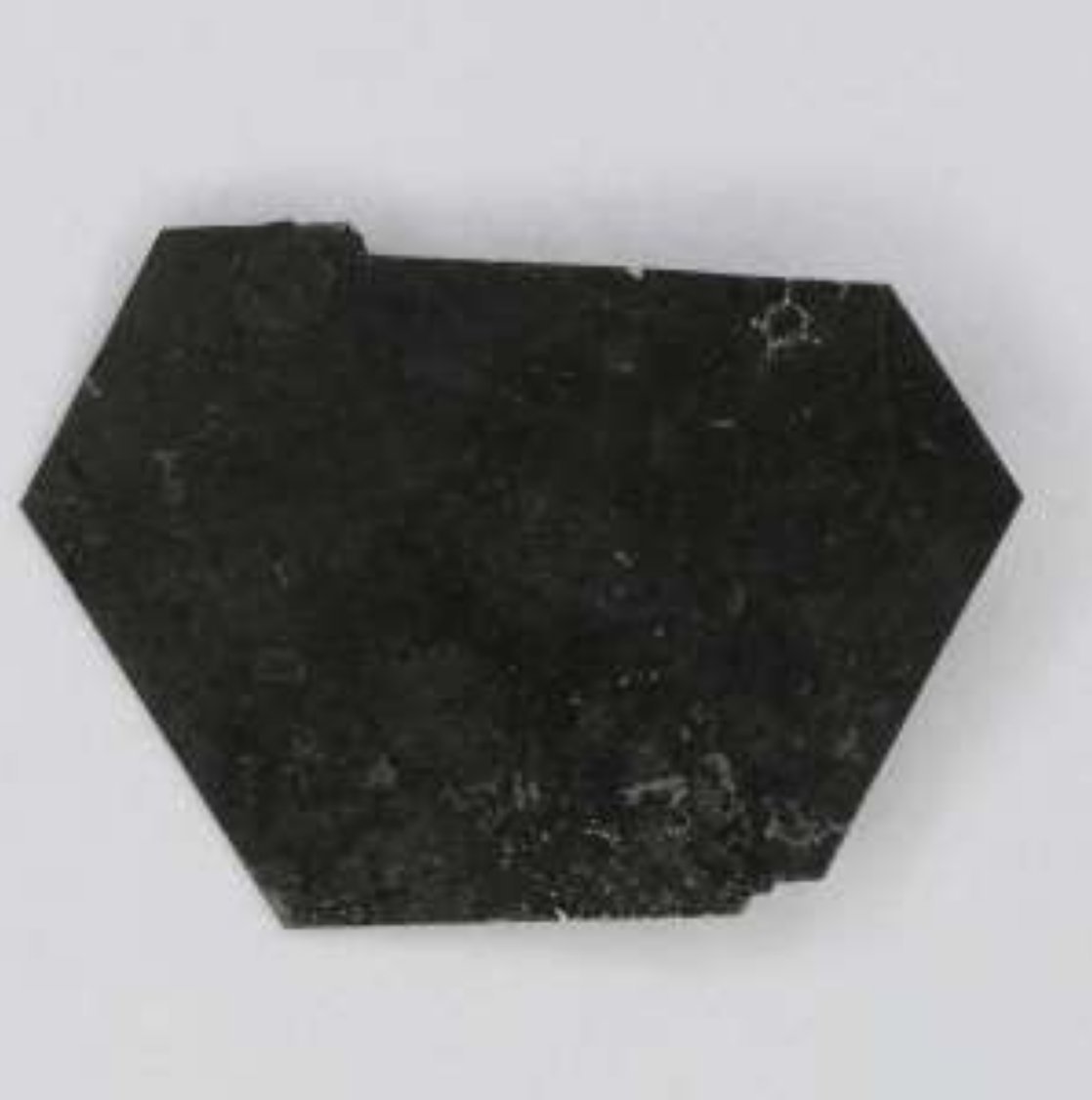
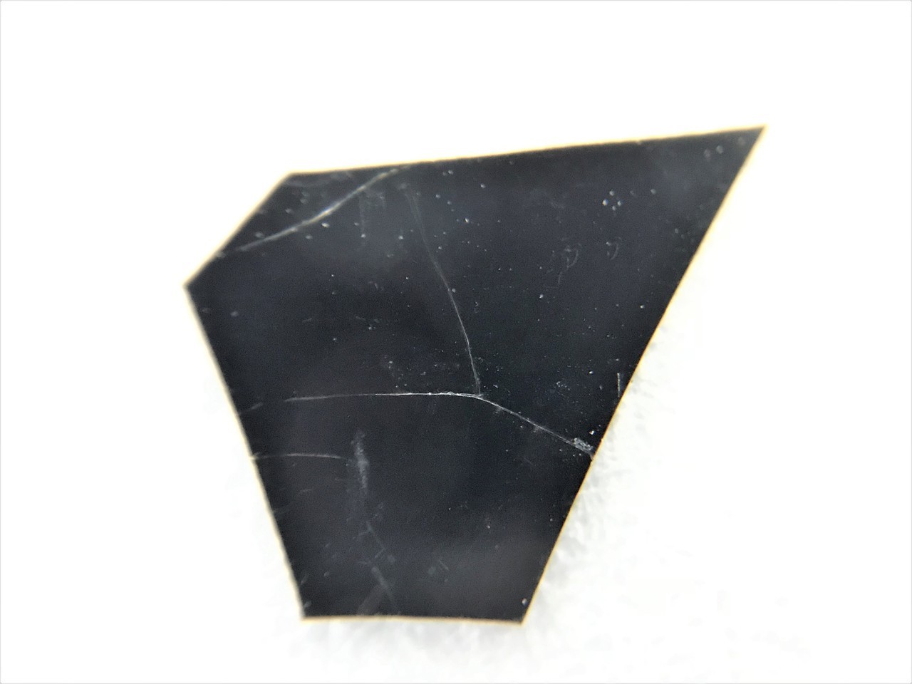
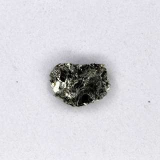
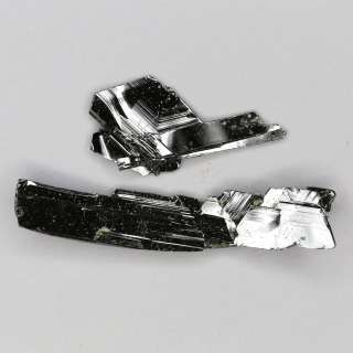
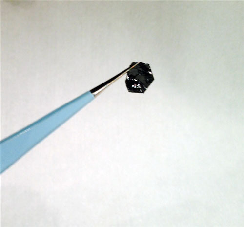
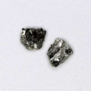
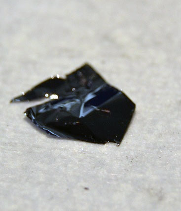
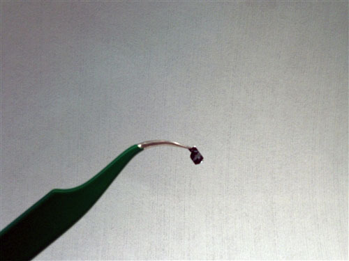
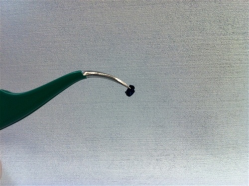
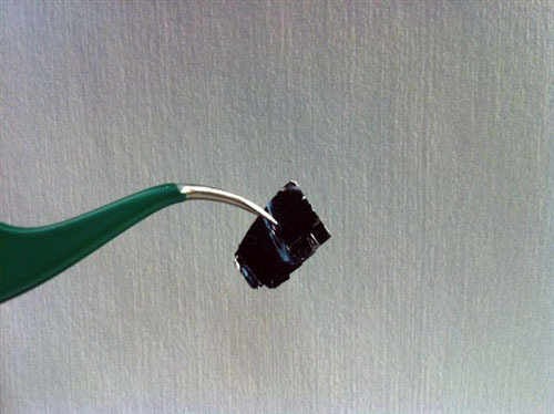
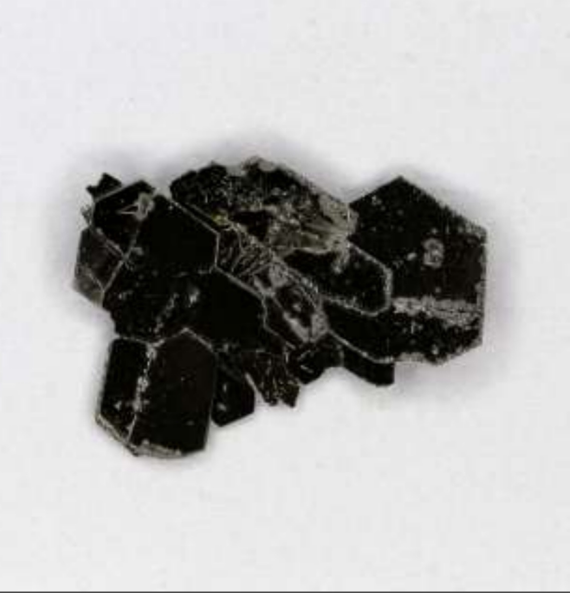
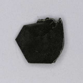
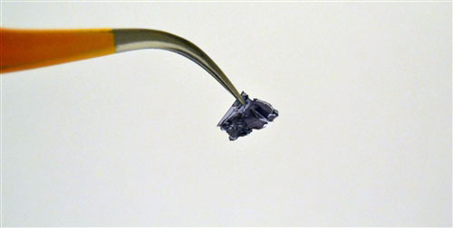
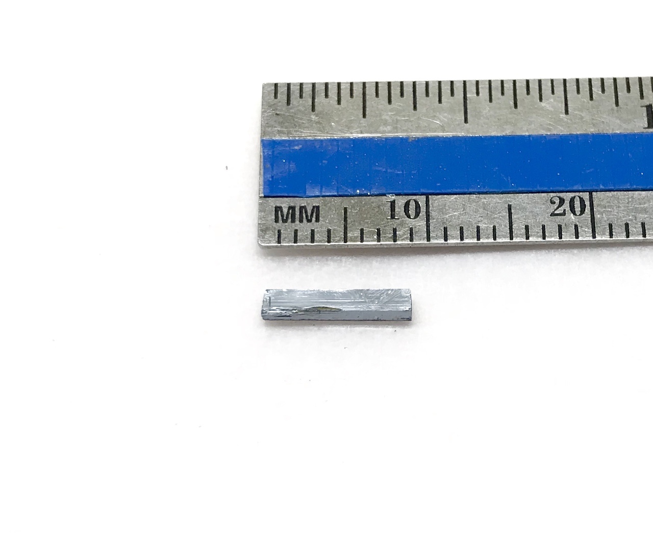
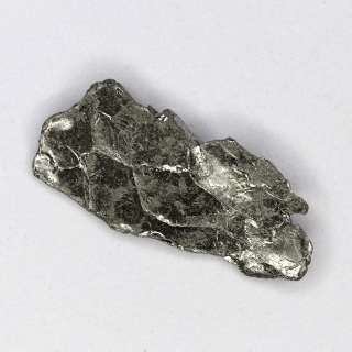
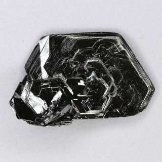
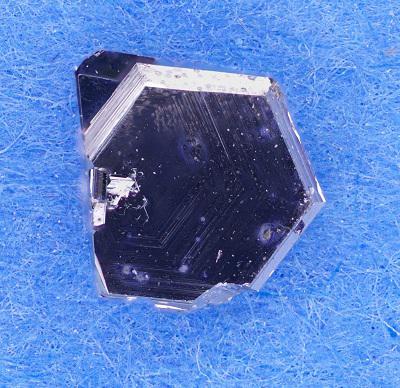
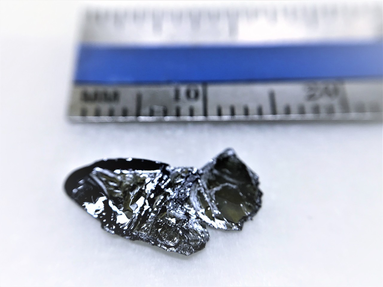
  • TiTe2 二碲化钛晶体 (Titanium Ditelluride)
    Similar to graphene and MoS2, TiTe? is also layered material (layered transition metal dichalcogenide) crystallizing in the 1T-CdI2 structure. It is a semimetal but very small gap (~50-100 meV) opens up as a result of charge density waves (CDW) formation.Owing to weak interlayer couple can be isolated to monolayers on variety substrates. From few- to monolayers, TiTe? possesses various interesting physical properties ranging from unusual - extraordinary Raman spectra and electrical conductivity. Each sample is characterized by various techniques such as electrical conductivity, Raman spectrum, XRD, XPS, AES, and ARPES to provide the highest quality samples for your research needs.Our TiTe2 crystals are stabilized in 2H-phase (semimetallic and CDW metallic phase). They are grown using two different techniques through chemical vapor transport (CVT) or flux zone growth (see description of these two methods below). These crystals are treated as gold standards in 2D materials field owing to perfected electronic behavior with guaranteed electronic response and low zero temperature resistance values. Our TiTe2 crystals exhibit low impurity resistance (zero temperature resistance), high carrier mobility, extremely clean and sharp XRD peaks, and negligible amount of defects (see published results as well as CVT vs. Flux based methods below ). TiTe2 crystals come ready for exfoliation without any preparation. If you research needs STM grade surfaces or even STM samples (TiTe2 mounted on conductive STM holders) please contact us, we will be happy to arrange these samples.Properties of vdW TiTe2 crystalsGrowth method matters Flux zone or CVT growth method? Contamination of halides and point defects in layered crystals are well known cause for their reduced electronic mobility, reduced anisotropic response, poor e-h recombination, low-PL emission, and lower optical absorption. Flux zone technique is a halide free technique used for synthesizing truly semiconductor gradevdW crystals. This method distinguishes itself from chemical vapor transport (CVT) technique in the following regard: CVT is a quick (~2 weeks) growth method but exhibits poor crystalline quality and the defect concentration reaches to 1E11 to 1E12 cm-2 range. In contrast, flux method takes long (~3 months) growth time, but ensures slow crystallization for perfect atomic structuring, and impurity free crystal growth with defect concentration as low as 1E9 - 1E10 cm-2. During check out just state which type of growth process is preferred. Unless otherwise stated, 2Dsemiconductors ships Flux zone crystals as a default choice.
  • 二碲化铂晶体 PtTe2(Platina Ditelluride)
    二碲化铂晶体 PtTe2(Platina Ditelluride)晶体尺寸:2~3毫米电学性能:金属,顺磁性晶体结构:六边形晶胞参数:a = b = 0.4000 nm, c = 0.5192 nm, α = β = 90°, γ = 120°晶体类型:合成晶体纯度:>99.995%Powder X-ray diffraction (XRD) of a single crystal PtTe2. X-ray diffraction was performed at room temperature using a D8 Venture Bruker. Stoichiometric analysis of a single crystal PtTe2 by Energy-dispersive X-ray spectroscopy (EDX).Raman spectrum of a single crystal PtTe2. Measurement was performed with a 785 nm Raman system at room temperature.
  • 二碲化钨晶体(99.995%) WTe2(Tungsten Ditelluride)
    二碲化钨晶体 WTe2(Tungsten Ditelluride) 晶体尺寸:10毫米电学性能:半金属,type II Weyl semimetal (WSM)晶体结构:斜方晶系 P晶胞参数:a = 0.348 nm, b = 0.625 nm, c = 1.405 nm, α = β = γ = 90°晶体类型:合成晶体纯度:>99.995%属性:半导体X-ray diffraction on a WTe2 single crystal aligned along the (001) plane. XRD was performed at room temperature using a D8 Venture Bruker. The 5 XRD peaks correspond, from left to right, to (00l) with l = 2, 4, 6, 8, 10 Powder X-ray diffraction (XRD) of a single crystal WTe2. X-ray diffraction was performed at room temperature using a D8 Venture Bruker. Stoichiometric analysis of a single crystal WTe2 by Energy-dispersive X-ray spectroscopy (EDX).Raman spectrum of a single crystal WTe2. Measurement was performed with a 785 nm Raman system at room temperature.
  • 二碲化钛
    简介:二维晶体材料指的是以石墨烯为代表的单原子层及少数原子层厚度的晶体材料,巨纳集团除了提供石墨烯材料、设备、检测等一体化服务外,还联合美国2D Semiconductors为全球客户提供高质量的二维晶体材料、粉体、溶液、薄膜等材料,并提供定制服务,以满足客户的不同需求。二碲化钛Titanium Ditelluride (TiTe?)
  • 二碲化钨
    简介:二维晶体材料指的是以石墨烯为代表的单原子层及少数原子层厚度的晶体材料,巨纳集团除了提供石墨烯材料、设备、检测等一体化服务外,还联合美国2D Semiconductors为全球客户提供高质量的二维晶体材料、粉体、溶液、薄膜等材料,并提供定制服务,以满足客户的不同需求。二碲化钨Tungsten Ditelluride (WTe?)
  • 二碲化钯晶体 PdTe2 (Palladium Ditelluride)
    二碲化钯晶体 PdTe2 (Palladium Ditelluride)晶体尺寸:2-3毫米电学性能:金属,半导体(Tc ~ 1.7K)晶体结构:六边形晶胞参数:a = b = 0.4035 nm, c = 0.5105 nm, α = β = 90°, γ = 120°晶体类型:合成晶体纯度:>99.995% Powder X-ray diffraction (XRD) of a single crystal PdTe2. X-ray diffraction was performed at room temperature using a D8 Venture Bruker. Stoichiometric analysis of a single crystal PdTe2 by Energy-dispersive X-ray spectroscopy (EDX). Raman spectrum of a single crystal PdTe2. Measurement was performed with a 785 nm Raman system at room temperature.
  • 二碲化钼
    简介:二维晶体材料指的是以石墨烯为代表的单原子层及少数原子层厚度的晶体材料,巨纳集团除了提供石墨烯材料、设备、检测等一体化服务外,还联合美国2D Semiconductors为全球客户提供高质量的二维晶体材料、粉体、溶液、薄膜等材料,并提供定制服务,以满足客户的不同需求。二碲化钼MoTe?
  • 二碲化锆
    简介:二维晶体材料指的是以石墨烯为代表的单原子层及少数原子层厚度的晶体材料,巨纳集团除了提供石墨烯材料、设备、检测等一体化服务外,还联合美国2D Semiconductors为全球客户提供高质量的二维晶体材料、粉体、溶液、薄膜等材料,并提供定制服务,以满足客户的不同需求。二碲化锆ZrTe?
  • 二碲化锡
    简介:二维晶体材料指的是以石墨烯为代表的单原子层及少数原子层厚度的晶体材料,巨纳集团除了提供石墨烯材料、设备、检测等一体化服务外,还联合美国2D Semiconductors为全球客户提供高质量的二维晶体材料、粉体、溶液、薄膜等材料,并提供定制服务,以满足客户的不同需求。二碲化锡Tin ditelluride (SnTe?)
  • 二碲化钴
    简介:二维晶体材料指的是以石墨烯为代表的单原子层及少数原子层厚度的晶体材料,巨纳集团除了提供石墨烯材料、设备、检测等一体化服务外,还联合美国2D Semiconductors为全球客户提供高质量的二维晶体材料、粉体、溶液、薄膜等材料,并提供定制服务,以满足客户的不同需求。二碲化钴CoTe?
  • 碲化镓
    简介:二维晶体材料指的是以石墨烯为代表的单原子层及少数原子层厚度的晶体材料,巨纳集团除了提供石墨烯材料、设备、检测等一体化服务外,还联合美国2D Semiconductors为全球客户提供高质量的二维晶体材料、粉体、溶液、薄膜等材料,并提供定制服务,以满足客户的不同需求。碲化镓Gallium Telluride (GaTe)
  • 二碲化铌晶体(99.995%) NbTe2(Niobium Selenide)
    二碲化铌晶体 NbTe2(Niobium Selenide) 晶体尺寸:~8毫米电学性能:金属,半导体(TC ~ 0.7k)晶体结构:单斜晶系,C晶胞参数:a=1.470 nm,b=0.364,c=0.935 nm,α=γ=90°,β=108°晶体类型:合成晶体纯度:>99.995% X-ray diffraction on a NbTe2 single crystal aligned along the (101) plane. XRD was performed at room temperature using a D8 Venture Bruker. The 4 XRD peaks correspond, from left to right, to (h 0 l), with h = l = 1, 2, 3, 4Powder X-ray diffraction (XRD) of a single crystal NbTe2. X-ray diffraction was performed at room temperature using a D8 Venture Bruker. Stoichiometric analysis of a single crystal NbTe2 by Energy-dispersive X-ray spectroscopy (EDX).Raman spectrum of a single crystal NbTe2. Measurement was performed with a 785 nm Raman system at room temperature.
  • 碲化锌晶体(ZnTe)
    碲化锌晶体(ZnTe) 尺寸: 5 x 5 x 0.1 mm-20 x 20 x 10 mm各个尺寸晶向:110表面处理: 抛光、镀膜、非镀膜应用:THz探测、THz产生 主要型号及尺寸列表:110 Orientation SIZE5 x 5 x 0.2 mm10 x 10 x 0.2 mm15 x 15 x 1 mm20 x 20 x 0.5 mm5 x 5 x 0.5 mm10 x 10 x 0.5 mm15 x 15 x 2 mm20 x 20 x 0.8 mm5 x 5 x 1mm10 x 10 x 1 mm 15 x 15 x 3 mm20 x 20 x 1 mm5 x 5 x 2 mm10 x 10 x 1.5 mm15 x 15 x 4 mm20 x 20 x 2 mm5 x 5 x 3 mm10 x 10 x 2 mm15 x 15 x 5 mm 5 x 5 x 4 mm10 x 10 x 3 mm  5 x 5 x 5 mm10 x 10 x 4 mm   10 x 10 x 5 mm  CHIPS - Are normally based upon ZnTe 100 Substrate @ 0.5 - 1 mm thickness onto which is optically glued ZnTe 110 top wafer.110 Front Face SIZE RANGE110 300 - 500 um110 100 - 200 um110 40 - 90 um110 20 um5 x 5 mm5 x 5 mm5 x 5 mm5 x 5 mm10 x 10 mm10 x 10 mm10 x 10 mm10 x 10 mm110 10 um   5 x 5 mm10 x 10 mmPlano – Wedged SIZE RANGE110 20 - 40 um wedge110 20 - 40 um wedge110 20 - 40 um wedge110 20 - 40 um wedgewith 0.5 - 1.0 mm 100 substratewith 2mm 100 substratewith 4mm 100substratewith 6mm 100 substrate5 x 5 mm5 x 5 mm5 x 5 mm5 x 5 mm10 x 10 mm   注: 还有多种型号可选,也可以为您量身定做,详细的技术指标请向我公司咨询.
  • 二碲化铪晶体(99.995%) HfTe2(Hafnium Telluride)
    二碲化铪晶体 HfTe2(Hafnium Telluride)晶体尺寸:~10毫米电学性能:半金属晶体结构:六边形晶胞参数:a = b = 0.395 nm, c = 0.666 nm, α = β = 90°, γ = 120°晶体类型:合成晶体纯度:>99.995% X-ray diffraction on a HfTe2 single crystal aligned along the (001) plane. XRD was performed at room temperature using a D8 Venture Bruker. The 6 XRD peaks correspond, from left to right, to (00l) with l = 1, 2, 3, 4, 5, 6Powder X-ray diffraction (XRD) of a single crystal . X-ray diffraction was performed at room temperature using a D8 Venture Bruker. Stoichiometric analysis of a single crystal by Energy-dispersive X-ray spectroscopy (EDX).Raman spectrum of a single crystal . Measurement was performed with a 785 nm Raman system at room temperature.
  • SnTe2 二碲化硒晶体 (Tin ditelluride)
    Environmentally stable, perfect, World record size single crystal SnTe? (Tin diselenide) crystals are developed at our facilities using state-of-art techniques. All the crystals are ready to exfoliate as shown in the images. Crystals are larger than 1cm in size giving you plenty of material to work with. In the bulk form SnTe?2 is ~0.6-0.7 eV band gap semiconductor. Displays remarkable and unusual optical, mechanical, and electrical properties that are waiting to the published in the literature. Yet, monolayer SnTe? remains unknown by the scientific community and waiting to be discovered. Each crystal comes with full characterization.
  • 二碲化钼
    分类:半导体中文名称:二碲化钼英文名称:MoTe?纯度:≥99.9999%尺寸:~6 mm-10 mm
  • InTe 碲化铟晶体 (Indium Telluride)
    The only commercially available layered InTe crystals. In the bulk form (InTe), Indium Telluride, has band-gap at around 0.6 eV and display strong photoluminescence. Similar to molybdenum disulfide, it has layered structure (lamellar) with weak interlayer coupling, enabling to isolate down to monolayers. InTe crystals exhibit TlSe-like structural transformation and thus has 2D anisotropic response much similar to ReS2, WTe2, and TiS3. Each monolayer is four atoms thick (Te-In-In-Te) that is roughly 0.9-1.0 nm. In our facilities, we have isolated InTe down to monolayer. In the literature, monolayer InTe is currently under-studied, yet to be discovered. Raman peaks are sharp and strong indicating high crystallinity. Our crystals are grown by state-of-the-art growth techniques after 5 weeks and show high crystallinity. The size of the samples is typically around ~4mm in size. InTe has a layered structure with weak interlayer coupling. Single crystal InTe comes ready for exfoliation and is ideal for 2D research.Properties of InTe layered crystals - 2Dsemiconductors USA
  • 碲化铋硫化物
    简介:二维晶体材料指的是以石墨烯为代表的单原子层及少数原子层厚度的晶体材料,巨纳集团除了提供石墨烯材料、设备、检测等一体化服务外,还联合美国2D Semiconductors为全球客户提供高质量的二维晶体材料、粉体、溶液、薄膜等材料,并提供定制服务,以满足客户的不同需求。碲化铋硫化物Bismuth Telluride Sulfide (Bi?Te?.?S?.?)
  • 碲化锡 Sb2Te3 (Antimony Telluride)
    晶体尺寸:10毫米电学性能:半导体,拓扑绝缘体,热电性晶体结构:六边形晶胞参数:a = b = 0.425nm,C = 3.048nm,α=β= 90°γ= 120晶体类型:合成晶体纯度:>99.995%表征方法:XRD、拉曼、EDXX-ray diffraction on a Sb2Te3 single crystal aligned along the (001) plane. XRD was performed at room temperature using a D8 Venture Bruker. The 7 XRD peaks correspond, from left to right, to (00l) with l = 6, 9, 12, 15, 18, 21, 24 Powder X-ray diffraction (XRD) of a single crystal Sb2Te3. X-ray diffraction was performed at room temperature using a D8 Venture Bruker.Stoichiometric analysis of a single crystal Sb2Te3 by Energy-dispersive X-ray spectroscopy (EDX).Raman spectrum of a single crystal Sb2Te3. Measurement was performed with a 785 nm Raman system at room temperature.
  • 二碲化钼晶体(99.995%) 2H-MoTe2(Molybdenum Ditelluride)
    二碲化钼晶体 2H-MoTe2(Molybdenum Ditelluride)晶体尺寸:~10毫米电学性能:N型半导体晶体结构:六边形晶胞参数:a = b = 0.353 nm, c = 1.396 nm, α = β = 90, γ = 120°晶体类型:合成晶体纯度:>99.995% X-ray diffraction on a MoTe2 single crystal aligned along the (001) plane. XRD was performed at room temperature using a D8 Venture Bruker. The 4 XRD peaks correspond, from left to right, to (00l) with l = 2, 4, 6, 8Powder X-ray diffraction (XRD) of a single crystal MoTe2. X-ray diffraction was performed at room temperature using a D8 Venture Bruker. Stoichiometric analysis of a single crystal 2H MoTe2 by Energy-dispersive X-ray spectroscopy (EDX).Raman spectrum of a single crystal 2H MoTe2. Measurement was performed with a 785nm Raman system at room temperature.
  • ZnTe Crystal_碲化锌晶体_Zinc telluride THZ晶体_筱晓光子
    THZ生成晶体 碲化锌晶体-现货供应Semiconductor THz Crystals: ZnTe (Zinc Telluride)crystals with 110 orientation are used for THz generation by optical rectification process. Optical rectification is a difference frequency generation in media with large second order susceptibility. For femtosecond laser pulses which have large bandwidth the frequency components interact with each other and their difference produce bandwidth from 0 to several THz. Detection of the THz pulse occurs via free-space electro-optic detection in another 110 oriented ZnTe crystal. The THz pulse and the visible pulse are propagated collinearly through the ZnTe crystal. The THz pulse induces a birefringence in ZnTe crystal which is read out by a linearly polarized visible pulse. When both the visible pulse and the THz pulse are in the crystal at the same time, the visible polarization will be rotated by the THz pulse. Using a λ/4 waveplate and a beamsplitting polarizer together with a set of balanced photodiodes, it is possible to map THz pulse amplitude by monitoring the visible pulse polarization rotation after the ZnTe crystal at a variety of delay times with respect to the THz pulse. The ability to read out the full electric field, both amplitude and delay, is one of the attractive features of time-domain THz spectroscopy. ZnTe are also used for IR optical components substrates and vacuum deposition. NOTE: ZnTe crystal contains micro bubbles and they are visible in projection of illuminated crystal. However this does not affect the THz generation. We do not accept complains on presence of bubbles in crystal.GaSe (Gallium Selenide) crystals used for THz generation shows a large bandwidth of up to 41 THz. GaSe is a negative uniaxial layered semiconductor with a hexagonal structure of 62 m point group and a direct bandgap of 2,2 eV at 300 K. GaSe crystal features high damage threshold, large nonlinear optical coefficient (54 pm/V), suitable transparent range, and low absorption coefficient, which make it an alternative solution for broadband mid infrared electromagnetic waves generation. Due to broadband THz generation and detection using a sub-20 fs laser source, GaSe emitter-detector system performance is considered to achieve comparable or even better results than using thin ZnTe crystals. In order to achieve frequency selective THz wave generation and detection system, GaSe crystals of appropriate thickness should be used. NOTE: because of material structure it is possible to cleave GaSe crystal along (001) plane only. Another disadvantage is softness and fragility of GaSe. Micophotons delivery time: from 5 - 6 days
  • ZrTe2 二碲化锆晶体
    ZrTe2 belongs to group-IV TMDCs family and adopts a stable 1T-octahedral structure. ZrTe2' s eelectronic bandstructure has interesting characteristics showing crossings of valence and conduction bands, near the Fermi level suggesting topological 3D Dirac semimetal behavior [1]. Interestingly, DFT calculations have also shown opening of electronic band gap for sheets below 3-4 layers, and becomes direct gap semiconductor in monolayer form (Egap~0.3-0.5 eV). These ZrTe2 crystals were designed and optimized at our facilities starting 2014 to achieve perfect electronic grade materials with: 1) excellent stoichiometry, 2) large single domain size, 3) single phase materials without any mixed phases or amorphous content, 4) unmatched purity -electronic grade (5.8N), 99.9998% confirmed. Our crystals exhibit sharpest Raman and XRD peaks in the commercial market proving the high quality of our materials.purity.Properties of ZrTe2 layered crystals Growth method matters Flux zone or CVT growth method? Contamination of halides and point defects in layered crystals are well known cause for their reduced electronic mobility, reduced anisotropic response, poor e-h recombination, low-PL emission, and lower optical absorption. Flux zone technique is a halide free technique used for synthesizing truly semiconductor grade vdW crystals. This method distinguishes itself from chemical vapor transport (CVT) technique in the following regard: CVT is a quick (~2 weeks) growth method but exhibits poor crystalline quality and the defect concentration reaches to 1E11 to 1E12 cm-2 range. In contrast, flux method takes long (~3 months) growth time, but ensures slow crystallization for perfect atomic structuring, and impurity free crystal growth with defect concentration as low as 1E9 - 1E10 cm-2. During check out just state which type of growth process is preferred. Unless otherwise stated, 2Dsemiconductors ships Flux zone crystals as a default choice.
  • 二硒化钨晶体(99.995%) WSe2(Tungsten Diselenide)-N型
    二硒化钨晶体 WSe2(Tungsten Diselenide)-P型晶体尺寸:~10毫米电学性能:半导体,P型晶体结构:六边形晶胞参数:a = b = 0.328 nm, c = 1.298 nm, α = β = 90°, γ = 120°晶体类型:合成晶体纯度:>99.995%X-ray diffraction on a WSe2 single crystal aligned along the (001) plane. XRD was performed at room temperature using a D8 Venture Bruker. The 5 XRD peaks correspond, from left to right, to (00l) with l = 2, 4, 6, 8, 10Powder X-ray diffraction (XRD) of a single crystal WSe2. X-ray diffraction was performed at room temperature using a D8 Venture Bruker.Stoichiometric analysis of a single crystal WSe2 by Energy-dispersive X-ray spectroscopy (EDX).Raman spectrum of a single crystal WSe2. Measurement was performed with a 785 nm Raman system at room temperature.
  • TlGaTe2 碲化镓铊晶体
    The only commercially available TlGaTe2 vdW crystals have been synthesized at our facilities through float zone technique. TlGaTe2 semiconductors belong to the thallium chalcogenides family with the chemical formula TlBX2 (where B=In or Ga, X=S, Se or Te). Members of this family have both layered (TlGaSe2, TlGaS2, TlInS2) and chain (TlInSe2, TlInTe2, TlGaTe2) structures. Stacking of the atoms in TlGaSe2, TlGaS2 and TlInS2 layered crystals is arranged in the form of two twisted anionic layers with the weak bonded Tl(+1) cations located in the trigonal cavities between them. Recently, low-temperature rhombohedral orderedphase of Tl-based III–V–VI2 ternary chalcogenides has been predicted to be topologically nontrivial and a terminated surface with a single Dirac cone has been identified through first-principles calculations (Phys. Rev. Lett. 105, 036404). TlGaTe2 crystals exhibit anisotropic structural, electronic, and optical properties with the band gap of 1.2 eV.Properties of TlGaTe2 layered crystals by 2Dsemiconductors USA
  • 二碲化钼(MoTe2)
    1、企业介绍泰州巨纳新能源有限公司:巨纳集团(Sunano Group)是能源行业的知名品牌。泰州巨纳新能源有限公司(Sunano Energy)是国内最早的从事石墨烯制备、性能检测及应用产品开发的公司之一,注册资本11000万元,有办公用房300多平方米,厂房和洁净室3000多平方米。核心研发团队主要由国内外知名高校博士组成,部分成员来自于2010年诺贝尔物理学奖小组,项目技术处于国际领先地位,在石墨烯领域拥有专利30余项。企业管理团队有丰富的成功创业经验,创新意识强,公司客户遍布全球。2、高质量二维晶体材料简介:二维晶体材料指的是以石墨烯为代表的单原子层及少数原子层厚度的晶体材料。巨纳集团除了提供石墨烯材料、设备、检测等一体化服务外,还联合荷兰HQ Graphene为全球客户提供高质量的类石墨烯二维晶体材料,并提供定制服务,以满足客户的不同需求。 名称:二碲化钼(MoTe2) 纯度:>99.995% 尺寸:~6 mm-10 mm 属性:半导体
  • Sb2Te3 碲化锑晶体
    Antimony telluride is a topological insulator with the chemical formula of Sb2Te3. It crystallizes in an orthorhombic space group. Our Sb2Te3 crystals measure centimeters in size, rated at 99.9999% purity, and exhibit strong and sharp Raman signal, ideal environmental stability, and high crystalline order. Crystals are synthesized through flux zone technique to achieve extremely high crystallinity for advanced research applications and fundamental research projects.Sb2Te3 single crystal characteristics
Instrument.com.cn Copyright©1999- 2023 ,All Rights Reserved版权所有,未经书面授权,页面内容不得以任何形式进行复制