基于二氧化硅衬底的全区域覆盖的单层二硫化钼
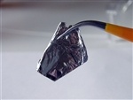
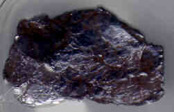
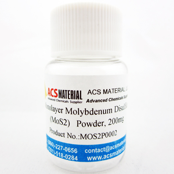
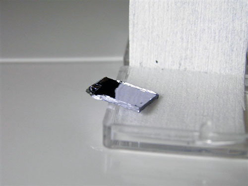
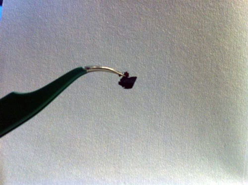
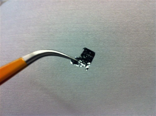
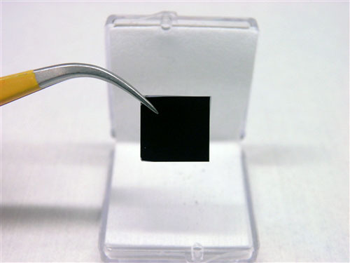
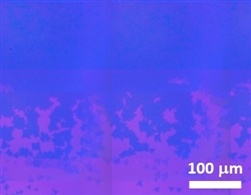
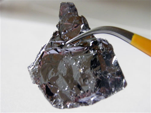
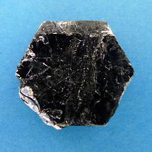
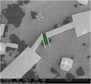
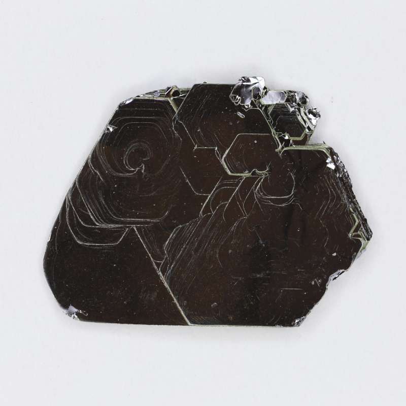
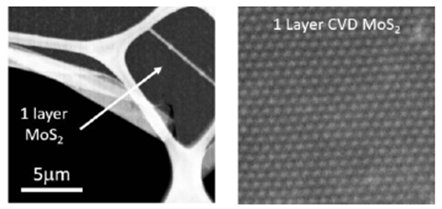
This product contains full area coverage MoS2 monolayers on SiO2/Si substrates. Sample size measures 1cm in size and the entire sample surface contains monolayer thick MoS2 sheet. Synthesized full area coverage monolayer MoS2 is highly luminescent and Raman spectroscopy studies also confirm the monolayer thickness. In comparison to full area coverage MoS2 on sapphire, full area coverage MoS2 on SiO2/Si display higher PL intensity.Sample Properties. Sample size1cm x 1cm square shapedSubstrate typeThermal oxide (SiO2/Si) substrates CoverageFull Coverage MonolayerElectrical properties1.85 eV Direct Bandgap SemiconductorCrystal structure Hexagonal PhaseUnit cell parametersa = b = 0.313 nm, c = 1.230 nm,α = β = 90°, γ = 120°Production method Atmospheric Pressure Chemical Vapor Deposition (APCVD)Characterization methodsRaman, photoluminescence, TEM, EDSSpecifications1) Identification. Full coverage 100% monolayer MoS2 uniformly covered across SiO2/Si substrates.2) Physical dimensions. One centimeter in size. Larger sizes up to 2-inch wafer-scale available upon requests.3) Smoothness. Atomically smooth surface with roughness 0.2 nm.4) Uniformity. Highly uniform surface morphology. MoS2 monolayers uniformly cover across the SiO2/Si substrates. 5) Purity. 99.9995% purity as determined by nano-SIMS measurements6) Reliability. Repeatable Raman and photoluminescence response7) Crystallinity. High crystalline quality, Raman response, and photoluminescence emission comparable to single crystalline monolayer flakes.8) Substrate. SiO2/Si substrates. But our research and development team can transfer MoS2 monolayers onto variety of substrates including PET and quartz without significantcompromisation of material quality.9) Defect profile. MoS2 monolayers do not contain intentional dopants or defects. However, our technical staff can produce defected MoS2 using α-bombardment technique.Supporting datasets [for 100% Full area coverage on SiO2/Si]Transmission electron images (TEM) acquired from CVD grown full area coverage MoS2 monolayers on SiO2/Si confirming highly crystalline nature of monolayers Energy dispersive X-ray spectroscopy (EDX) characterization on CVD grown full area coverage MoS2 on SiO2/Si confirming Mo:S 1:2 ratios Room temperature photoluminescence spectroscopy (PL) and Raman spectroscopy (Raman) measurements performed on CVD grown full area coverage MoS2 monolayers on SiO2/Si. Raman spectroscopy measurement confirm monolayer nature of the CVD grown samples and PL spectrum display sharp and bright PL peak located at 1.85 eV in agreement with the literature.


 我要推广仪器
 下载APP
下载APP