当前位置: 仪器信息网 > 行业主题 > >

森另覆盖率

仪器信息网森另覆盖率专题为您整合森另覆盖率相关的最新文章,在森另覆盖率专题,您不仅可以免费浏览森另覆盖率的资讯, 同时您还可以浏览森另覆盖率的相关资料、解决方案,参与社区森另覆盖率话题讨论。

森另覆盖率相关的耗材

  • Millex-FA针式过滤装置
    Millex-FA针式过滤装置, 1.0 µ m,亲水性PTFE,50 mm,HB-HB所有产品、耗材配件均原厂,公司拥有完善的质量管理体系和专业的技术团队,在全国多个城市设立服务机构,覆盖率广,高效率、响应速度快!除销售仪器、配件耗材外,还可提供维修、维保、培训等一站式产品和服务解决方案!
  • 基于蓝宝石衬底的全区域覆盖的单层二硒化锡
    This product contains full area coverage SnSe2 monolayers on c-cut sapphire substrates. Sample size measures 1cm in size and the entire sample surface contains monolayer thick SnSe2 sheet. Synthesized full area coverage monolayer SnSe2 is highly crystalline, some regions also display significant crystalline anisotropy.Sample Properties.Sample size1cm x 1cm square shapedSubstrate typeSapphire c-cut (0001) CoverageFull monolayer coverageElectrical properties 1.5 eV Indirect Gap SemiconductorCrystal structureHexagonal PhaseUnit cell parametersa = b = 0.380, c = 0.612 nm,α = β = 90°, γ = 120°Production method Low Pressure Chemical Vapor Deposition (LPCVD)Characterization methodsRaman, angle resolved Raman spectroscopy,photoluminescence, absorption spectroscopy TEM, EDSSpecifications 1) Identification. Full coverage 100% monolayer SnSe2 uniformly covered across c-cut sapphire2) Physical dimensions. One centimeter in size. Larger sizes up to 2-inch wafer-scale available upon requests.3) Smoothness. Atomically smooth surface with roughness 0.15 nm.4) Uniformity. Highly uniform surface morphology. SnSe2 monolayers uniformly cover across the sample. 5) Purity. 99.9995% purity as determined by nano-SIMS measurements6) Reliability. Repeatable Raman and photoluminescence response7) Crystallinity. High crystalline quality, Raman response, and photoluminescence emission comparable to single crystalline monolayer flakes.8) Substrate. c-cut Sapphire but our research and development team can transfer SnSe2 monolayers onto variety of substrates including PET, quartz, and SiO2/Si without significant compromisation of material quality.9) Defect profile. SnSe2 monolayers do not contain intentional dopants or defects. However, our technical staff can produce defected SnSe2 using α-bombardment technique. Supporting datasets [for 100% Full area SnSe2 monolayers on c-cut Sapphire] Transmission electron images (TEM) acquired from CVD grown full area coverage SnSe2 monolayers on c-cut sapphire confirming high crystallinityEnergy dispersive X-ray spectroscopy (EDX) characterization on CVD grown full area coverage monolayer SnSe2 on c-cut sapphire Raman spectroscopy measurement confirm monolayer nature of the CVD grown samples and shows the high crystallinity of the CVD samples. PL spectrum does not show any PL signal due to indirect band nature.
  • 上海森谱As-1-4有色金属院空心阴极灯Ag银 Al铝 As砷 Ba钡 Ca钙 Cd镉
    上海森谱As-1-4有色金属院空心阴极灯Ag银 Al铝 As砷 Ba钡 Ca钙 Cd镉北京普析、海光、华洋、浩天晖瀚时、东西分析、上海精科、上海仪电、皖仪、天瑞、森谱、天美、上海光谱、美析、福立、沈分、华光、中和测通、原子吸收,AS-1-4型号 有北分瑞利、北京普析、海光、华洋、浩天晖瀚时、东西分析、上海精科、上海仪电、皖仪、天瑞、森谱、天美、上海光谱、美析、福立、沈分、华光、中和测通、原子吸收元素有:Ag银、Al铝、As砷、Au金、B硼、Ba钡、Be铍、Bi铋、Ca钙、Cd镉、Co钴、Cr铬、Cu铜、Fe铁、Ga镓、Ge锗、Hg汞、K钾、Li锂、Mg镁、Mn锰、Mo、钼Na钠、Ni镍、Pb铅、Pd钯、Pt铂、Rb铷、Re铼、Rh铑、Ru钌、Sb锑、Sc钪、Se硒、Sn锡、Sr锶、Ta钽、Te碲、Ti钛、Tl铊、W钨、V钒、Y钇、Zn锌、Zr锆上海森谱As-1-4有色金属院空心阴极灯Ag银 Al铝 As砷 Ba钡 Ca钙 Cd镉欢迎订购产 品 能 参 数 ★起辉电压:≦360V,起辉电压低(特别是用高频率点灯时如此),可以适用于各种不同的原子吸收光谱仪(AAS),一般原子吸收光谱仪灯的供电频率是200Hz、400Hz或更高,每秒钟灯要连续接通断开数百次。★最大工作电流:一般在10~30mA之间,AS-2型空心阴极灯略大。★超纯光谱性能:特征辐射谱线强度高而稳定,没有阴极材料杂质元素或其他元素、阳极材料、充入的惰性气体等发射谱线的重叠干扰,持续而稳定光源输出。★发射性能:独特的阴极环系统,保证达到均匀快速的发光性能。★噪  声:<0.3%,信号噪音降低到最小。★背  景:在特征谱线两侧的辐射背景低,主要分析线附近的背景强度小于分析强度的1%。★预热时间:<30min,一般在5-15min之间。★稳定性:≦+1%—-1%铜灯在30min内基线漂移<1%,其他元素灯在5min内基线漂移<1%。★灯体结构:基底的特殊设计保证了阴极针和接线的直接连接,结构紧凑,牢固可靠,使用方便。★寿  命:气体容量空间比其他品牌产品更大,产品使用寿命更长,一般元素灯≥5000mA.h,易熔、易挥发元素灯≥3000mA.h,可长期存放。如果您想对我们的产品进一步了解,请咨询客服,我们将以优惠的价格、 高品质的产品回报客户、我们期待您的来电!
  • Symmetry色谱柱
    Symmetry色谱柱当化学家为制药与生物制药产品开发分析方法时,选择具有重现能力的HPLC柱至关重要。被选择的色谱柱需要在这个新的药物产品的整个生命周期中都能提供一致的色谱分析结果。而Symmetry色谱柱显示出跨越多年的卓越重现性。确保重现性是我们在供应Symmetry色谱柱时的第一要素。如此优秀的重现性,则来自于我们持续不懈的致力于HPLC色谱柱行业内最严格的指标控制。Symmetry色谱柱,由高纯硅胶、严格控制的生产工艺和色谱柱装填工艺所得,为色谱工作者提供最好的、最重现的HPLC色谱柱。我们的目标是为您提供您可赖以获得可靠、耐用的色谱方法的柱家族。Symmetry柱可帮助您增加实验室的产率、并允许全球实验室之间的方法转移更方便可靠。固定相性质一览表填料 键合相 粒径 颗粒形状 孔径 碳载量 封端Symmetry C 18 3.5, 5, 7 μm 球形 100 19% 是 C 8 3.5, 5, 7 μm 球形 100 12% 是SymmetryShield RP18 3.5, 5, 7 μm 球形 100 17% 是 RP8 3.5, 5, 7 μm 球形 100 15% 是窄指标范围的优势Symmetry色谱柱具有行业内最窄的配体表面覆盖率指标。表面覆盖率(配体密度)是影响重现性的最重要的参数之一。此处展示了表面覆盖率的小差异对阿米替林/二氢苊的相对选择因子指标的影响。窄的色谱柱指标为色谱工作者带来重现性方面的优势。因为Symmetry柱具有行业内最窄的配体表面覆盖率指标,这使得Symmtry能提供最小的分离度漂移,以及更好的批与批间、柱与柱间重现性。窄的指标范围确保更小的选择因子α漂移较小的α漂移可减少对峰分离度的改变C 18 配体表面覆盖率指标范围
  • PMMA覆盖石墨烯
    参数:表面电阻:小于600Ω/sq定制:<300Ω/sq透明度: 95%Parameter:Sheet Resistance: 600Ω/sqCustom Order: 300Ω/sqTransparency: 95%
  • 悬浮在横向电磁场网格上的单层石墨烯薄膜
    由化学蒸气沉淀形成,转移到多碳孔支持膜横向电磁场的网格上,石墨烯悬浮没有底层,比碳孔高2微米。石墨烯薄膜生长方法:CVD合成、转移方法:干净转移,质量控制:光学显微镜、拉曼光谱、扫描电镜和透射电镜批签,大小:3毫米,外观(颜色):透明,透明度:97%,外观(形状):薄,覆盖率:95%,石墨烯层数:1,厚度(原理上):0.345毫微米,场效应管电子AI203迁移率:2,800cm2/Vs,场效应管SIO2/SI的电子迁移率:3,500cm2/Vs,表面电阻:170欧姆平方米,晶粒尺寸:约10μm,横向电磁场网格:类型:多孔碳支持膜 ?R2/4,孔大小:2微米,孔间距:4微米,孔直径:3毫米,涂层:镀金。
  • Waters  氘灯组件
    ACQUITY PDA/TUV 2489/2998 PERFORMANCE MAINTENANCE KIT产品介绍:1. 具有智能芯片技术,包含所有可使您的仪器每年保持最佳性能所需的Waters高质量零部件。 2. 适用范围:①ACQUITY UPLC PDA检测器; ②ACQUITY eLambda PDA检测器; ③ACQUITY UPLC TUV检测器; 3. 性能维护组件包括以下部件:氘灯一个(性能优,长寿命)。所有产品、耗材配件均原厂,公司拥有完善的质量管理体系和专业的技术团队,在全国多个城市设立服务机构,覆盖率广,高效率、响应速度快!除销售仪器、配件耗材外,还可提供维修、维保、培训等一站式产品和服务解决方案!
  • Waters 氘灯组件
    TUV Detector Performance Maintenance Kit产品介绍:1.TUV性能维护组件包含所有可使您的仪器每年保持最佳性能所需的Waters高质量零部件2. 适用范围:①2487 Dual Wavelength Absorbance检测器; ②2488 Multichannel Absorbance检测器; ③ACQUITY TUV检测器(序列号K05UPT699N或更新版本);3. 性能维护组件包括以下部件:氘灯一个(性能优,长寿命)。所有产品、耗材配件均原厂,公司拥有完善的质量管理体系和专业的技术团队,在全国多个城市设立服务机构,覆盖率广,高效率、响应速度快!除销售仪器、配件耗材外,还可提供维修、维保、培训等一站式产品和服务解决方案!
  • 弗氏不完全佐剂
    弗氏不完全佐剂liquid别名:FICA应用弗氏佐剂可用于产生免疫原的油包水乳剂。油包水乳剂中的抗原可刺激高且持久的抗体应答,而这可归因于抗原的缓慢释放。弗氏(不完全)佐剂缺乏在弗氏完全佐剂中发现的分枝杆菌,因此它可以最大限度地减少副作用。它用于增强注射。它用于乳化注射到动物体内的抗原,从而抗血清中产生单克隆抗体。包装10, 10, 10 mL其他说明每毫升含 0.85mL 石蜡油和 0.15mL 二缩甘露醇一油酸。所有产品、耗材配件均原厂,公司拥有完善的质量管理体系和专业的技术团队,在全国多个城市设立服务机构,覆盖率广,效率高、响应速度快!除销售仪器、配件耗材外,还可提供维修、维保、培训等一站式产品和服务解决方案!
  • 北京绿百草科技供应GH GEL ODS-C18亲水填料
    北京绿百草科技供应GHGEL ODS-C18亲水填料关键词:GHGEL ODS填料,亲水填料,C18填料北京绿百草科技供应GH GEL ODS-C18亲水填料,有10&mu m 、50&mu m的不同规格。GH GEL ODS-C18填料,是完全球型、表面光滑的多孔硅胶,具有非常高的表面键合覆盖率。GH GEL ODS-C18采用专利封端技术,对酸性和碱性以及螯合物具有优越的分离性能,机械稳定性好,是各种不同性质有机化合物分离的理想选择。GH GEL ODS-C18填料广泛用于各种医药中间体的提取和纯化,产品性价比高。
  • Waters氘灯组件
    PDA/TUV Performance Maintenance Kit产品介绍:1. 配备智能芯片技术,包含所有可使您的仪器每年保持最佳性能所需的Waters高质量零部件。 2. 适用范围:①ACQUITY UPLC PDA检测器; ②ACQUITY eLambda PDA检测器; ③ACQUITY UPLC TUV检测器(采用智能芯片技术); 3. 性能维护组件包括以下部件:氘灯一个(性能优,长寿命)。所有产品、耗材配件均原厂,公司拥有完善的质量管理体系和专业的技术团队,在全国多个城市设立服务机构,覆盖率广,高效率、响应速度快!除销售仪器、配件耗材外,还可提供维修、维保、培训等一站式产品和服务解决方案!
  • 基于蓝宝石衬底的全区域覆盖的单层二硒化铼
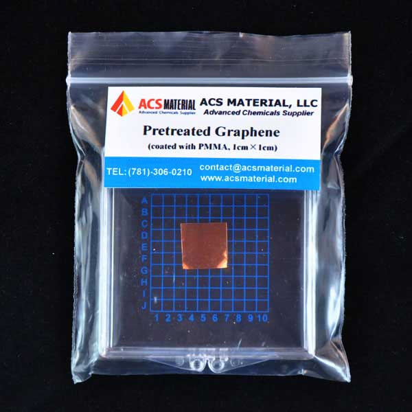
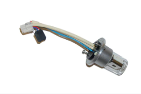
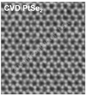
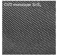
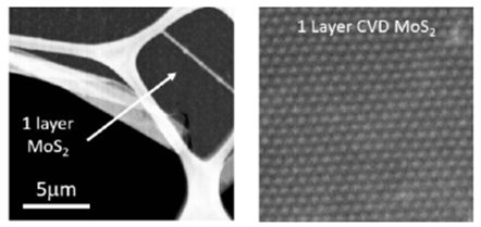
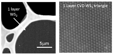
    This product contains full area coverage ReSe2 monolayers on c-cut sapphire substrates. Sample size measures 1cm in size and the entire sample surface contains monolayer thick ReSe2 sheet. Synthesized full area coverage monolayer ReSe2 is highly crystalline, some regions also display significant crystalline anisotropy. Sample Properties.Sample size1cm x 1cm square shapedSubstrate typeSapphire c-cut (0001)CoverageFull monolayer coverageElectrical properties1.45 eV Anisotropic Semiconductor (Indirect Bandgap)Crystal structure Distorted Tetragonal Phase (1T’)Unit cell parametersa = 0.656 nm, b = 0.672 nm, c = 0.674 nm,α = 91.74°, β = 105°, γ = 119°Production methodAtmospheric Pressure Chemical Vapor Deposition (APCVD)Characterization methodsRaman, angle resolved Raman spectroscopy,photoluminescence, absorption spectroscopy TEM, EDSSpecifications1) Identification. Full coverage 100% monolayer ReSe2 uniformly covered across c-cut sapphire 2) Physical dimensions. One centimeter in size. Larger sizes up to 2-inch wafer-scale available upon requests.3) Smoothness. Atomically smooth surface with roughness 0.15 nm.4) Uniformity. Highly uniform surface morphology. ReSe2 monolayers uniformly cover across the sample.5) Purity. 99.9995% purity as determined by nano-SIMS measurements6) Reliability. Repeatable Raman and photoluminescence response7) Crystallinity. High crystalline quality, Raman response, and photoluminescence emission comparable to single crystalline monolayer flakes.8) Substrate. c-cut Sapphire but our research and development team can transfer ReSe2 monolayers onto variety of substrates including PET,quartz, and SiO2/Si without significant compromisation of material quality.Defect profile. ReSe2 monolayers do not contain intentional dopants or defects. However, our technical staff can produce defected ReSe2 using α-bombardment technique.Supporting datasets [for 100% Full area ReSe2 monolayers on c-cut Sapphire] Transmission electron images (TEM) and angle resolved Raman spectroscopy measurements acquired from CVD grown full area coverage ReSe2 monolayers on c-cut sapphire confirming crystalline anisotropyEnergy dispersive X-ray spectroscopy (EDX) characterization on CVD grown full area coverage monolayer ReSe2 on c-cut sapphireRaman spectroscopy measurement confirm monolayer nature of the CVD grown samples. Differential reflectance measurements clearly show band gap at 1.45 eV for monolayer ReS2 consistent with the existing literature values. PL spectrum does not show any PL signal due to indirect band nature.
  • 于蓝宝石衬底的全区域覆盖的单层二硒化钨
    This product contains full area coverage WSe2 monolayers on c-cut sapphire substrates. Sample size measures 1cm in size and the entire sample surface contains monolayer thick WSe2 sheet. Synthesized full area coverage monolayer WSe2 is highly luminescent and Raman spectroscopy studies also confirm the monolayer thickness (please see the technical specifications)Sample Properties.Sample size1cm x 1cm square shapedSubstrate typeSapphire c-cut (0001)CoverageFull monolayer coverageElectrical properties 1.62 eV Direct Bandgap SemiconductorCrystal structureHexagonal PhaseUnit cell parametersa= b = 0.327 nm, c = 1.295 nm, α = β = 90°, γ = 120°Production methodLow pressure Chemical Vapor Deposition (LPCVD)Characterization methodsRaman, photoluminescence, TEM, EDS Specifications1) Identification. Full coverage 100% monolayer WSe2 uniformly covered across c-cut sapphire2) Physical dimensions. One centimeter in size. Larger sizes up to 2-inch wafer-scale available upon requests.3) Smoothness. Atomically smooth surface with roughness 0.15 nm.4) Uniformity. Highly uniform surface morphology. WSe2 monolayers uniformly cover across the sample.5) Purity. 99.9995% purity as determined by nano-SIMS measurements6) Reliability. Repeatable Raman and photoluminescence response7) Crystallinity. High crystalline quality, Raman response, and photoluminescence emission comparable to single crystalline monolayer flakes.8) Substrate. c-cut Sapphire but our research and development team can transfer WSe2 monolayers onto variety of substrates including PET, quartz, and SiO2/Si without significant compromisation of material quality.9) Defect profile. WSe2 monolayers do not contain intentional dopants or defects. However, our technical staff can produce defected WSe2 using α-bombardment technique.Supporting datasets [Full area coverage monolayer WSe2 on c-cut Sapphire]Transmission electron images (TEM) acquired from CVD grown full area coverage WSe2 monolayers on c-cut sapphire confirming highly crystalline nature of monolayersRoom temperature photoluminescence spectroscopy (PL) and Raman spectroscopy (Raman) measurements performed on CVD grown full area coverage monolayer WSe2 on c-cut sapphire. Raman spectroscopy measurement confirm monolayer nature of the CVD grown samples and PL spectrum display sharp and bright PL peak located at 1.67 eV in agreement with the literature.
  • Alltech Adsorbosphere色谱柱
    Alltech Adsorbosphere色谱柱 Adsorbosphere &bull 高温键合,独特的表面覆盖率、稳定性和重现性 &bull 球形,全端基封尾 对于需要特殊填料表面和特殊的稳定性的应用,需要选择Adsorbosphere® 柱。高温键合25-40%的硅羟基到固定相上,这比用标准的低温键合要键合的多。端基封尾和单体键合降低了不同批次色谱柱间的差异性。端基封尾硅羟基的所占比例比使用其他材料形成稳定键合相要大。端基封尾会因为水解而失效,但选择性却变化很小,因为封尾点所占整个固定相的比例很小。奥泰Adsorbosphere® CN-AQ 柱是氰基固定相,主要用于分离三环的抗抑郁药(TCA&rsquo s)。 Adsorbosphere HS色谱柱 &bull 高碳覆盖率,球形C18填料,耐腐蚀性流动相 &bull 高表面积 Adsorbosphere HS能耐腐蚀性的流动相。高密度键合到高表面积的球形硅胶上,C18碳覆盖率达到20%。这种不易被水浸润的固定相保护了硅胶不会被腐蚀性流动相所破坏,如象离子对试剂和缓冲盐,从而延长了柱子的使用寿命,对有机化合物有很高的选择性。 Adsorbosphere UHS色谱柱 &bull 非常高的表面积,形成非常特殊的键合固定相 &bull 对于需要高分离度的应用,这是非常理想的选择 Adsorbosphere UHS C18柱是奥泰表面积最大的载体(30% 碳覆盖率),主要用于需要高分离的应用中,如象对结构类似的化合物的分离。这种例子包括多环芳烃的分离(EPA法610),对二氨基联苯的分离(EPA法605),以及一些结构接近的化合物的分离,包括维生素D2、D3、PTH氨基酸和各种化学异构体的分离。
  • WTW SenTix 940 pH电极
    WTW IDS数字式pH电极IDS探头将完善测量技术与先进科技结合于一身高级优化的探头技术与最先进的电子测量技术相结合QSC功能实时评估IDS pH探头状态IDS探头自主储存序列号和校准历史——即插即用IDS电导率测量:两支探头全范围覆盖IDS pH探头SenTix® 940*SenTix® 940-3SensoLyt® 900-P*SenTix® 950*SenTix® 980*SenTix® ORP 900*SensoLyt® ORP 900-P*pH测量范围0.000 – 14.000 ± 0.0042.000 – 12.000 ± 0.0040.000 – 14.000 ± 0.004mV: ±1200.0 ± 0.2温度范围0 – 80 ℃0 – 80 ℃0 – 60 ℃0 – 80 ℃0 – 100 ℃0 – 100 ℃0 – 60 ℃参考电解质胶体胶体聚合物3 mol/l KCl3 mol/l KCl3 mol/l KCl聚合物膜形圆柱型圆柱型圆柱型圆柱型锥型-圆柱型隔膜纤维纤维孔洞陶瓷铂丝陶瓷孔洞轴材质塑料塑料玻璃塑料玻璃玻璃玻璃轴尺寸长120 mm ± 2 mm,直径12 mm ± 0.5 mm* 可选择无线模式电极(-P),参数与带电缆电极相同,可连接无线模块订购信息103740SenTix® 940IDS pH 复合电极,带凝胶电解质,塑料杆和集成温度传感器。QSC 功能。电极包括 1.5 m 固定电缆,带防水数字连接器。用于 MultiLine® ,MonoLine,inoLab® IDS。103741SenTix® 940 -3IDS pH 复合电极,带凝胶电解质,塑料杆和集成温度传感器。QSC 功能。电极包括 3 m 固定电缆,带防水数字连接器。用于 MultiLine® ,MonoLine 和 inoLab® IDS。
  • 基于蓝宝石衬底的全区域覆盖的少层二硒化铂
    This product contains full area coverage PtSe2 layers (single/multi) on c-cut sapphire substrates. Sample size measures 1cm in size and the entire sample surface contains PtSe2 sheets. Synthesized full area coverage PtSe2 is highly crystalline, some regions also display significant crystalline anisotropy.Sample Properties.Sample size1cm x 1cm square shapedSubstrate typeSapphire c-cut (0001)CoverageFull coverage (mostly few-layers)Electrical properties Semi-metalCrystal structure Hexagonal PhaseUnit cell parametersa = b = 0.372 nm, c = 0.508 nm,α = β = 90°, γ = 120°Production methodLow Pressure Chemical Vapor Deposition (LPCVD)Characterization methodsRaman, angle resolved Raman spectroscopy,photoluminescence, absorption spectroscopy TEM, EDSSpecifications1) Identification. Full coverage 100% monolayer PtSe2 uniformly covered across c-cut sapphire2) Physical dimensions. One centimeter in size. Larger sizes up to 2-inch wafer-scale available upon requests.3) Smoothness. Atomically smooth surface with roughness 0.15 nm.4) Uniformity. Highly uniform surface morphology. PtSe2 monolayers uniformly cover across the sample. 5) Purity. 99.9995% purity as determined by nano-SIMS measurements6) Reliability. Repeatable Raman and photoluminescence response7) Crystallinity. High crystalline quality, Raman response, and photoluminescence emission comparable to single crystalline monolayer flakes.8) Substrate. c-cut Sapphire but our research and development team can transfer PtSe2 monolayers onto variety of substrates including PET, quartz, and SiO2/Si without significant compromisation of material quality.9) Defect profile. PtSe2 monolayers do not contain intentional dopants or defects. However, our technical staff can produce defected PtSe2 using α-bombardment technique.Supporting datasets [for 100% Full area PtSe2 monolayers on c-cut Sapphire] Transmission electron images (TEM) acquired from CVD grown full area coverage PtSe2 monolayers on c-cut sapphire confirming high crystallinityRaman spectroscopy measurement confirm monolayer nature of the CVD grown samples and shows the high crystallinity of the CVD samples. PL spectrum does not show any PL signal due to indirect band nature.
  • WTW SenTix ORP-T 900 ORP电极
    WTW IDS数字式电极IDS探头将完善测量技术与先进科技结合于一身高级优化的探头技术与最先进的电子测量技术相结合QSC功能实时评估IDS pH探头状态IDS探头自主储存序列号和校准历史——即插即用IDS电导率测量:两支探头全范围覆盖IDS pH探头SenTix® 940*SenTix® 940-3SensoLyt® 900-P*SenTix® 950*SenTix® 980*SenTix® ORP-T 900*SensoLyt® ORP 900-P*pH测量范围0.000 – 14.000 ± 0.0042.000 – 12.000 ± 0.0040.000 – 14.000 ± 0.004mV: ±1200.0 ± 0.2温度范围0 – 80 ℃0 – 80 ℃0 – 60 ℃0 – 80 ℃0 – 100 ℃0 – 100 ℃0 – 60 ℃参考电解质胶体胶体聚合物3 mol/l KCl3 mol/l KCl3 mol/l KCl聚合物膜形圆柱型圆柱型圆柱型圆柱型锥型-圆柱型隔膜纤维纤维孔洞陶瓷铂丝陶瓷孔洞轴材质塑料塑料玻璃塑料玻璃玻璃玻璃轴尺寸长120 mm ± 2 mm,直径12 mm ± 0.5 mm* 可选择无线模式电极(-P),参数与带电缆电极相同,可连接无线模块。
  • 基于蓝宝石衬底的全区域覆盖的单层二硫化锡
    This product contains full area coverage SnS2 monolayers on c-cut sapphire substrates. Sample size measures 1cm in size and the entire sample surface contains monolayer thick SnS2 sheet. Synthesized full area coverage monolayer SnS2 is highly crystalline, some regions also display significant crystalline anisotropy.Sample Properties.Sample size1cm x 1cm square shapedSubstrate typeSapphire c-cut (0001)CoverageFull monolayer coverageElectrical properties 2.2 eV Indirect Gap SemiconductorCrystal structureHexagonal PhaseUnit cell parametersa = b = 0.362, c = 0.590 nm,α = β = 90°, γ = 120°Production method Low Pressure Chemical Vapor Deposition (LPCVD)Characterization methodsRaman, angle resolved Raman spectroscopy,photoluminescence, absorption spectroscopy TEM, EDSSpecifications1) Identification. Full coverage 100% monolayer SnS2 uniformly covered across c-cut sapphire2) Physical dimensions. One centimeter in size. Larger sizes up to 2-inch wafer-scale available upon requests.3) Smoothness. Atomically smooth surface with roughness 0.15 nm.4) Uniformity. Highly uniform surface morphology. SnS2 monolayers uniformly cover across the sample. 5) Purity. 99.9995% purity as determined by nano-SIMS measurements6) Reliability. Repeatable Raman and photoluminescence response7) Crystallinity. High crystalline quality, Raman response, and photoluminescence emission comparable to single crystalline monolayer flakes.8) Substrate. c-cut Sapphire but our research and development team can transfer SnS2 monolayers onto variety of substrates including PET, quartz, and SiO2/Si without significant compromisation of material quality.9) Defect profile. SnS2 monolayers do not contain intentional dopants or defects. However, our technical staff can produce defected SnS2 using α-bombardment technique.Supporting datasets [for 100% Full area SnS2 monolayers on c-cut Sapphire] Transmission electron images (TEM) acquired from CVD grown full area coverage SnS2 monolayers on c-cut sapphire confirming high crystallinity Energy dispersive X-ray spectroscopy (EDX) characterization on CVD grown full area coverage monolayer SnS2 on c-cut sapphireRaman spectroscopy measurement confirm monolayer nature of the CVD grown samples and shows the high crystallinity of the CVD samples. PL spectrum does not show any PL signal due to indirect band nature.
  • 基于二氧化硅衬底的全区域覆盖的单层二硫化钼
    This product contains full area coverage MoS2 monolayers on SiO2/Si substrates. Sample size measures 1cm in size and the entire sample surface contains monolayer thick MoS2 sheet. Synthesized full area coverage monolayer MoS2 is highly luminescent and Raman spectroscopy studies also confirm the monolayer thickness. In comparison to full area coverage MoS2 on sapphire, full area coverage MoS2 on SiO2/Si display higher PL intensity.Sample Properties. Sample size1cm x 1cm square shapedSubstrate typeThermal oxide (SiO2/Si) substrates CoverageFull Coverage MonolayerElectrical properties1.85 eV Direct Bandgap SemiconductorCrystal structure Hexagonal PhaseUnit cell parametersa = b = 0.313 nm, c = 1.230 nm,α = β = 90°, γ = 120°Production method Atmospheric Pressure Chemical Vapor Deposition (APCVD)Characterization methodsRaman, photoluminescence, TEM, EDSSpecifications1) Identification. Full coverage 100% monolayer MoS2 uniformly covered across SiO2/Si substrates.2) Physical dimensions. One centimeter in size. Larger sizes up to 2-inch wafer-scale available upon requests.3) Smoothness. Atomically smooth surface with roughness 0.2 nm.4) Uniformity. Highly uniform surface morphology. MoS2 monolayers uniformly cover across the SiO2/Si substrates. 5) Purity. 99.9995% purity as determined by nano-SIMS measurements6) Reliability. Repeatable Raman and photoluminescence response7) Crystallinity. High crystalline quality, Raman response, and photoluminescence emission comparable to single crystalline monolayer flakes.8) Substrate. SiO2/Si substrates. But our research and development team can transfer MoS2 monolayers onto variety of substrates including PET and quartz without significantcompromisation of material quality.9) Defect profile. MoS2 monolayers do not contain intentional dopants or defects. However, our technical staff can produce defected MoS2 using α-bombardment technique.Supporting datasets [for 100% Full area coverage on SiO2/Si]Transmission electron images (TEM) acquired from CVD grown full area coverage MoS2 monolayers on SiO2/Si confirming highly crystalline nature of monolayers Energy dispersive X-ray spectroscopy (EDX) characterization on CVD grown full area coverage MoS2 on SiO2/Si confirming Mo:S 1:2 ratios Room temperature photoluminescence spectroscopy (PL) and Raman spectroscopy (Raman) measurements performed on CVD grown full area coverage MoS2 monolayers on SiO2/Si. Raman spectroscopy measurement confirm monolayer nature of the CVD grown samples and PL spectrum display sharp and bright PL peak located at 1.85 eV in agreement with the literature.
  • 基于蓝宝石衬底的全区域覆盖的单层二硫化钨
    This product contains full area coverage WS2 monolayers on c-cut sapphire substrates. Sample size measures 1cm in size and the entire sample surface contains monolayer thick WS2 sheet. Synthesized full area coverage monolayer WS2 is highly luminescent and Raman spectroscopy studies also confirm the monolayer thickness.Sample Properties.Sample size1cm x 1cm square shapedSubstrate type(0001) c-cut sapphireCoverageFull coverage monolayerElectrical properties2.0 eV Direct Bandgap SemiconductorCrystal structureHexagonal PhaseUnit cell parametersa = b = 0.312 nm, c = 1.230 nm, α = β = 90, γ = 120°Production methodLow pressure Chemical Vapor Deposition (LPCVD)Characterization methodsRaman, photoluminescence, TEM, EDSSpecifications1) Identification. Full coverage 100% monolayer WS2 uniformly covered across c-cut sapphire 2) Physical dimensions. One centimeter in size. Larger sizes up to 2-inch wafer-scale available upon requests.3) Smoothness. Atomically smooth surface with roughness 0.2 nm.4) Uniformity. Highly uniform surface morphology. WS2 monolayers uniformly cover across the sample.5) Purity. 99.9995% purity as determined by nano-SIMS measurements 6) Reliability. Repeatable Raman and photoluminescence response7) Crystallinity. High crystalline quality, Raman response, and photoluminescence emission comparable to single crystalline monolayer flakes.8) Substrate. c-cut Sapphire but our research and development team can transfer WS2 monolayers onto variety of substrates including PET, quartz, and SiO2/Si without significant compromisation of material quality. 9) Defect profile. WS2 monolayers do not contain intentional dopants or defects. However, our technical staff can produce defected WS2 using α-bombardment technique.Supporting datasets [for 100% Full area WS2 coverage on c-cut Sapphire] Transmission electron images (TEM) acquired from CVD grown full area coverage WS2 monolayers on c-cut sapphire confirming highly crystalline nature of monolayersEnergy dispersive X-ray spectroscopy (EDX) characterization on CVD grown full area coverage monolayer WS2 on c-cut sapphire confirming W:S 1:2 ratios Room temperature photoluminescence spectroscopy (PL) and Raman spectroscopy (Raman) measurements performed on CVD grown full area coverage WS2 monolayers on c-cut sapphire. Raman spectroscopy measurement confirm monolayer nature of the CVD grown samples and PL spectrum display sharp and bright PL peak located at 2.00 eV in agreement with the literature.
  • 品牌系列色谱柱
    我公司提供以下品牌色谱柱:美国 LabAlliance 生产的 LabAlliance 系列瑞典 Nobel Eka 公司生产的 Kromasil 系列SMT 原装色谱柱蛋白分析柱色谱柱SMT原装色谱柱单层自聚合(SAM)技术 PH:1-12 SMT(美国分离技术公司)是最优秀的专业从事表面化学研究的公司。单层自聚合(SAM)技术使硅胶表面的功能配体密度更高,性能更好。较之传统的末端封装技术,应用了SAM技术的液相色谱柱更加经久耐用,适用条件更宽,适用范围更广泛。SMT采用专利的聚合技术使连接覆盖率接近100%。SMT的聚合技术使功能配体被间隔分子有效控制,这一过程保证了整体覆盖率和聚有机硅氧烷的高度交联。这使得固定相得到很好地保护,表现出对酸和碱性化合物前所未有的耐受性。独特的单层自聚合(SAM)技术 自组装单层自聚合(SAM)是超分子类似物,在某些方面表现出独特的优点。连接技术使有序的单功能分子层固定在固定相上,例如硅胶,氧化铝。这种连接技术被命名为水平聚合作用,这是由于Si-O-Si连接桥和硅胶底物是平行的。这是通过三功能性的烷基化试剂与硅胶底物在无水条件下的反应得到的。在色谱学中,根据被连接配体的长度,聚合化学可使单层覆盖率的厚度达到6-12的范围。例如,当C18配体被连接时,可以得到厚度为22的薄膜。在这一范围内的厚度保证了底物里和底物周围结合的配体没有小孔没有堵塞。并且通过核磁共振(NMR)表明了间隔分子式均匀分散在功能配体上的,而不是聚合在一起。SMT色谱柱的应用 用SMT-OuickSep Column检验低检测性的可卡因和尼古丁SMT-OuickSep C18 色谱柱在分离可卡因和尼古丁上有着显著地效果,使用普通有机流动相时,最小检测量可达1微微克。 用SMT相反色谱柱分离茶叶中的有效成分:儿茶素,咖啡因,表儿茶酸,表没食子儿,表儿茶素。
  • 佰氟达PFA三通扩口接头半导体清洗机配件
    在半导体清洗机中,PFA三通扩口接头作为一种重要的配件,其性能和品质对于整个清洗机的运行效果起着决定性的作用。针对这一关键配件,我们对其进行了深入研究和优化,以期在半导体清洗过程中实现更高的效率和更优质的清洗效果。  首先,我们采用了高品质的PFA材料制造这一接头。PFA,即全氟烷氧基聚合物,具有出色的化学稳定性和耐高温性能,能够在半导体清洗过程中抵抗各种化学试剂的侵蚀,确保接头的长期稳定运行。  其次,我们对PFA三通扩口接头的结构进行了精心设计。通过优化接头内部的流道设计,我们实现了更加顺畅的流体传输,提高了清洗液在半导体表面的覆盖率和冲洗效果。同时,扩口设计使得接头能够方便地与其他管道进行连接,提高了设备的整体安装效率和便利性。  此外,我们还注重接头的密封性能。在接头的设计和制造过程中,我们采用了先进的密封技术,确保接头在高压、高温等恶劣环境下仍能保持良好的密封效果,防止清洗液泄漏对设备造成损害。  最后,我们针对半导体清洗机的特殊需求,对PFA三通扩口接头进行了定制化生产。根据不同客户的清洗需求和设备配置,我们提供了多种规格和型号的接头供客户选择,以满足不同场景下的应用需求。  综上所述,通过优化PFA三通扩口接头的材质、结构、密封性能和定制化生产等方面,我们为半导体清洗机提供了更加可靠、高效的配件解决方案,助力半导体产业的快速发展。
  • 德国ORP电极SenTix ORP-T 900 货号:103791
    德国ORP电极SenTix ORP-T 900 货号:103791描述:铂 IDS ORP 电极,带液体电解质和玻璃杆,温度传感器。电极包括 1.5 m 带防水数字连接器的固定电缆,用于 MultiLine ,MonoLine undinoLab IDS,带3mol/ l KCl 滴管瓶。一、优点:1.高级优化的探头技术与先进的电子测量技术相结合;2.IDS探头自主储存序列号和校准历史-即插即用;3.QSC功能实时评估IDS pH探头状态;4.IDS电导率测量:两支探头全范围覆盖。 二、技术参数型号:SenTix ORP-T 900货号:103791量程范围:mV:±1200.0 ±0.2温度范围:0-100℃参考电解质:3mol/l KCL隔膜:陶瓷轴材质:玻璃轴尺寸:长120mm ±2mm,直径12mm ±0.5mm
  • 德国 ORP电极SenTix ORP-T 900 货号:103791
    德国ORP电极SenTix ORP-T 900 货号:103791描述:铂 IDS ORP 电极,带液体电解质和玻璃杆,温度传感器。电极包括 1.5 m 带防水数字连接器的固定电缆,用于 MultiLine ,MonoLine undinoLab IDS,带3mol/ l KCl 滴管瓶。一、优点:1.高级优化的探头技术与先进的电子测量技术相结合;2.IDS探头自主储存序列号和校准历史-即插即用;3.QSC功能实时评估IDS pH探头状态;4.IDS电导率测量:两支探头全范围覆盖。 二、技术参数型号:SenTix ORP-T 900货号:103791量程范围:mV:±1200.0 ±0.2温度范围:0-100℃参考电解质:3mol/l KCL隔膜:陶瓷轴材质:玻璃轴尺寸:长120mm ±2mm,直径12mm ±0.5mm
  • 赛默飞 Betasil Diol 色谱柱
    Betasil Diol 色谱柱• 2,3-二羟基丙基硅烷键合硅胶固定相• 正相分析常用色谱柱,亦可使用反相流动相• 高的表面覆盖率
  • 赛默飞 Betasil C6 色谱柱
    Betasil C6 色谱柱• 己烷基硅烷键合硅胶固定相• 疏水选择性比 C8 稍弱• 超高的表面覆盖率
  • Ultimate XB-Phenyl填料
    XB-Phenyl与直链烷烃选择性互补,同样采用超纯硅胶为基质,在硅胶上键合丙基苯基而成,具有高的表面覆盖率和完全双峰尾的特性,对芳香族化合物、极性化合物和难以分离的药物具有优良的分离效果。
  • 默克MERCK SPME 光纤支架
    SPME 光纤支架for use with manual sampling一般描述可调深度的套管可定位萃取头的取样位置,以及萃取头在 GC 进样口加热区的准确定位。萃取头可以锁定在暴露的位置。该支架可对包被的纤维进行保护,并控制在分析物在吸附和解吸附时的纤维暴露。该支持可无限次被重复利用并接受可替换的纤维束。 首次使用的用户必须同时订购支架和纤维束。用于手动进样的纤维支架可调节的深度指导可对用于进样的纤维进行定位并正确放置在GC注射口的加热区域。纤维可在暴露的位置进行锁定。用于自动化进样或HPLC分析的纤维支架可结合Varian 8100/8200 AutoSampler 或我们的SPME/HPLC接口使用该纤维支架。一款SPME升级试剂盒对于使用Varian AutoSampler进行操作是必需的-联系Varian仪器部门获取关于系统要求的更多信息。用于CTC CombiPAL/CombiPAL-xt及Gerstel MPS2的纤维支架所有产品、耗材配件均原厂,公司拥有完善的质量管理体系和专业的技术团队,在全国多个城市设立服务机构,覆盖率广,高效率、响应速度快!除销售仪器、配件耗材外,还可提供维修、维保、培训等一站式产品和服务解决方案!
  • 赛默飞Betasil C1 色谱柱
    Betasil C1 色谱柱• 三jia基硅烷键合硅胶固定相• 疏水选择性最弱的的反相色谱柱• 超高的表面覆盖率
  • 动态水分吸附仪-渗透率组件
    渗透率是薄膜类材料的重要特性,精确测量薄膜、纸张等的水分子渗透率对于评估其作为包装材料在不同水蒸汽分压环境下隔绝水分的功能有着重要的意义。 ProUmid公司生产的动态水分吸附仪可以选配一个渗透率组件,精确检测薄膜的渗透率。该渗透率组件有六个样品盘,可以同时测量5个薄膜(纸张)样品的渗透率,大大节省了试验时间。该仪器包括一个高灵敏度的天平和能够调节温湿度,气流循环的密闭空间。为渗透率的检测提供最理想的环境。 检测原理:将薄膜(纸张)覆盖在样品盘上,将盘内放置干燥剂、饱和食盐水溶液或水来制造一个与环境不同的水蒸汽分压,从而使水分子透过薄膜(纸张),迁移到达另一边。这种水分子的迁移可以通过称量样品盘的重量来检测。 这种方法结果非常准确,可以得到薄膜(纸张)材料的精确渗透率。特点:ProUmid公司生产的SPS和Vorp系列动态水分吸附仪能够精确的检测水蒸气透过薄膜的渗透率。仪器温湿度可调,可以模拟在范围非常广的环境条件下检测渗透率。仪器的称重精确度很高,可以检测低至0.05g/(m2 day)的渗透率。SPS和Vsorp系列动态水分吸附仪具备多样品高通量的特点,每次可同步检测5个样品,非常适合对比不同组成薄膜之间渗透性能的差异。
Instrument.com.cn Copyright©1999- 2023 ,All Rights Reserved版权所有,未经书面授权,页面内容不得以任何形式进行复制