当前位置: 仪器信息网 > 行业主题 > >

正电子偶素

仪器信息网正电子偶素专题为您整合正电子偶素相关的最新文章,在正电子偶素专题,您不仅可以免费浏览正电子偶素的资讯, 同时您还可以浏览正电子偶素的相关资料、解决方案,参与社区正电子偶素话题讨论。

正电子偶素相关的仪器

  • 正电子湮没寿命谱仪 400-860-5168转3524
    正电子湮没寿命谱仪:又名高分子材料分析仪 1930年Dirac从理论上预言了正电子的存在和1932年Anderson在观察宇宙线中发现了正电子之后,揭开了研究物质和反物质相互作用的序幕。1951年Deutsch发现了正电子和电子构成的束缚态—正电子素的存在更加深了对正电子物理的研究工作,同时,也开展了许多应用研究工作,形成了一门独立的课题正电子湮没谱学。 随着对正电子和正电子素及其与物质相互作用特性的深入了解,使正电子湮没技术在原子物理、分子物理、固态物理、表面物理、化学及生物学、医学等领域得到广泛应用,并取得独特的研究成果。它在诸如检验量子电动力学基本理论、研究弱相互作用、基本对称性及天体物理等基础科学中也发挥了重要作用。同时,随着人们对正电子湮没技术方法学上研究的深入进展,使这一门引人注目的新兴课题得到更快的发展。 实验用放射源22Na,其衰变纲图如右图所示。该源发生 衰变放出一个正电子后几乎同时(仅迟3 ps左右)还发射一个能量为1.28 MeV的 光子。因此,测量1.28 MeV的 光子与正电子湮没后放出的 光子(0.511 MeV)之间的时间间隔,就可得到正电子寿命。对每个湮没事件都可测得湮没过程所需时间。对足够多的湮没事件(~106个)进行统计,就可得到一个正电子湮没寿命谱。系统集成测试报告参数:系统时间分辨率(用50μCi 60Co源测量):保证值:≤ 200ps;典型值:≤ 180ps
    留言咨询
  • 正电子湮没寿命谱仪/正电子寿命皮秒定时系统positron annihilation lifetime产品简介 放射源发射出高能正电子射入物质中后,首先在极短时间内(约10-12ps以下)通过一系列非弹性碰撞减速,损失绝大部分能量至热能,这一过程称为注入与热化。热化后的正电子将在样品中进行无规扩散热运动,晶格中空位、位错等缺陷往往带有等效负电荷,由于库仑引力 正电子容易被这些缺陷捕获而停止扩散,并将在物质内部与电子发生湮没。从正电子射入物质到发生湮没所经历的时间一般称为正电子寿命。由于湮没是随机的,正电子湮没寿命只能从大量湮没事件统计得出。 正电子寿命谱仪性能特点正电子湮没技术对材料的结构相变和原子尺度的缺陷极为敏感,已经成为研究物质微观结构和电子结构的无损的探测分析手段。正电子湮没作为微观分析技术一种,其主要研究范围在于针对原子尺寸的微结构和缺陷。与通常的微观结构分析如STM、SEM、TEM等技术相比,正电子湮没技术不仅可以提供缺陷的尺寸信息、相变信息,而且可以提供缺陷随深度分布的信息,能够深入的分析材料的电子结构以及正电子湮没处的化学环境等,弥补了其他微观探测技术的不足,具有不可替代性。 应用领域1.金属材料的形变、疲劳、淬火、辐照、掺杂、氢损伤等在材料中造成的空位、位错、空位团等缺陷以及研究这些缺陷的退火效应。2.材料中相变过程,如合金中的沉淀现象、马氏体相变、非晶态材料中的晶化过程、离子固体中的相变、液晶及其他高分子材料,聚合物中的相变,凝聚态物理等3.研究固体的能带结构、费米面、空位形成能等4.研究材料的表面和表层结构和缺陷。 技术优势1.他对样品材料的种类几乎没有什么限制,可以是固体、液体或气体,可以是金属、半导体、绝缘体或高分子材料,可以是单晶、多晶或液晶等,适用于凡是与材料的电子密度及动量有关的问题。2.对样品温度没有限制,可以跨越材料的熔点或凝固点,而信息又是通过贯穿能力很强的γ射线携带而来,因此可以对样品做高低温的动态原位测量,测量时可施加电场、磁场、高气压、真空等特殊环境。3.研究样品中原子尺度的缺陷,如晶格中缺少一个或多个原子的缺陷,这些缺陷在电镜、X衍射中研究颇为困难。技术参数1.时间分辨率=120ps2.计数率1000cps,可自动计数3.自动能窗调节4.高压漂移,自动修正5.数据文件无需修改格式,可直接解谱6.小巧台式,安装环境要求低此外可提供正电子湮没辐射角关联、多普勒展宽谱、慢化正电子谱仪。
    留言咨询
  • 正电子湮没寿命谱仪:又名高分子材料分析仪 1930年Dirac从理论上预言了正电子的存在和1932年Anderson在观察宇宙线中发现了正电子之后,揭开了研究物质和反物质相互作用的序幕。1951年Deutsch发现了正电子和电子构成的束缚态—正电子素的存在更加深了对正电子物理的研究工作,同时,也开展了许多应用研究工作,形成了一门独立的课题正电子湮没谱学。 随着对正电子和正电子素及其与物质相互作用特性的深入了解,使正电子湮没技术在原子物理、分子物理、固态物理、表面物理、化学及生物学、医学等领域得到广泛应用,并取得独特的研究成果。它在诸如检验量子电动力学基本理论、研究弱相互作用、基本对称性及天体物理等基础科学中也发挥了重要作用。同时,随着人们对正电子湮没技术方法学上研究的深入进展,使这一门引人注目的新兴课题得到更快的发展。 实验用放射源22Na,其衰变纲图如右图所示。该源发生 衰变放出一个正电子后几乎同时(仅迟3 ps左右)还发射一个能量为1.28 MeV的 光子。因此,测量1.28 MeV的 光子与正电子湮没后放出的 光子(0.511 MeV)之间的时间间隔,就可得到正电子寿命。对每个湮没事件都可测得湮没过程所需时间。对足够多的湮没事件(~106个)进行统计,就可得到一个正电子湮没寿命谱。系统集成测试报告参数:系统时间分辨率(用50μCi 60Co源测量):保证值:≤ 200ps;典型值:≤ 180ps
    留言咨询
  • 正电子湮没寿命谱仪1.正电子湮没寿命谱仪应用于材料科学领域中半导体材料类缺陷的测试。这是一套测量设备和电源一体化的正电子湮没寿命谱仪。在寿命测试中,使用3GSPS来测算寿命时间,这是由两种BaF2 的闪烁体产生的高速脉冲信号所导入的。在多普勒宽谱(CDB)中,二维的柱图是由两个锗半导体探测器的波高分布特征值所计算出的。此外,这套正电子湮没寿命谱仪也可以用AMOC模式来测试相关材料的寿命时间及电子动量密度分布2.技术特征在寿命测试中,使用3GSPS来测算寿命时间,这是由两种BaF2 的闪烁体产生的高速脉冲信号所导入的。在多普勒宽谱(CDB)中,二维的柱图是由两个锗半导体探测器的波高分布特征值所计算出的。此外,这套测试设备也可以用AMOC模式来测试相关材料的寿命时间及电子动量密度分布3.技术原理时间分析光谱计、DSP多通道分析模块、前置放大器电源模块、高压电源模块、供电支架、BaF2闪烁体探测器、Ge半导体探测器、计算机PC、交换中心(每个模块PC和局域网电缆连接)4.应用案例四川大学中科院高能物理研究所日本各大高校研究所
    留言咨询
  • 高分子材料分析仪1930年Dirac从理论上预言了正电子的存在和1932年Anderson在观察宇宙线中发现了正电子之后,揭开了研究物质和反物质相互作用的序幕。1951年Deutsch发现了正电子和电子构成的束缚态—正电子素的存在更加深了对正电子物理的研究工作,同时,也开展了许多应用研究工作,形成了一门独立的课题正电子湮没谱学。随着对正电子和正电子素及其与物质相互作用特性的深入了解,使正电子湮没技术在原子物理、分子物理、固态物理、表面物理、化学及生物学、医学等领域得到广泛应用,并取得独特的研究成果。它在诸如检验量子电动力学基本理论、研究弱相互作用、基本对称性及天体物理等基础科学中也发挥了重要作用。同时,随着人们对正电子湮没技术方法学上研究的深入进展,使这一门引人注目的新兴课题得到更快的发展。实验用放射源22Na,其衰变纲图如右图所示。该源发生 衰变放出一个正电子后几乎同时(仅迟3 ps左右)还发射一个能量为1.28 MeV的 光子。因此,测量1.28 MeV的 光子与正电子湮没后放出的 光子(0.511 MeV)之间的时间间隔,就可得到正电子寿命。对每个湮没事件都可测得湮没过程所需时间。对足够多的湮没事件(~106个)进行统计,就可得到一个正电子湮没寿命谱。系统集成测试报告参数:系统时间分辨率(用50μCi 60Co源测量):保证值:≤ 200ps;典型值:≤ 180ps
    留言咨询
  • PSPB10000脉冲慢正电子束流装置 PSPB10000脉冲慢正电子束流是一种可精确调制时间、能量和位置的正电子束流,通过电磁线圈和电场的控制,可以实现对材料近表面和界面的结构形态进行分层扫描,可以实现材料中微观缺陷态的分层测量,从而对材料表面与界面进行结构表征。 从放射源产生的正电子首先通过慢化体能量降低到热能,然后通过聚束线圈实现对位置的调控,通过斩波器实现对时间的调控,通过加速电极实现对能量的调控。经过PSPB10000调制过的正电子可以停留在样品的特定深度。
    留言咨询
  • 正电子湮没寿命谱仪DPLS4000
    留言咨询
  • 数字化正电子湮没符合多普勒展宽谱仪
    留言咨询
  • 英国Allresist 正电子束光刻胶 AR-P 610系列描述-电子束,深紫外光(248nm)-最高分辨率,高对比度-对玻璃、硅和金属有很强的附着力-比PMMA敏感3-4倍-敏感性可以通过软烤调整-用于平面化和多层工艺-温度稳定,可达240℃-以甲基丙烯酸甲酯为基础的共聚物甲基丙烯酸,安全溶剂1-甲氧基-2-丙醇
    留言咨询
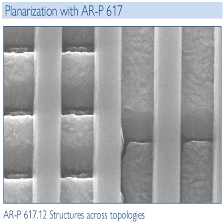
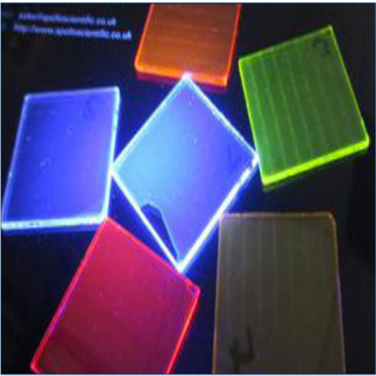
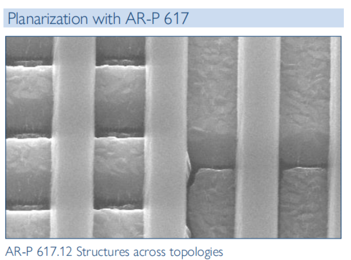
  • 产品详情 英国Allresist 正电子束光刻胶 AR-P 6200 (CSAR 62),高分辨率,用于生产集成电路和掩模的高对比度电子束电阻。 描述 -电子束 层thickn。0,05-1,6 evm (6000-1000 rpm)-高灵敏度,可通过开发人员-较高分辨率( 10nm)和非常高的对比度-工艺稳定性高,耐等离子体腐蚀-容易制造的起飞结构- poly(α-methyl styrene-co-α-chloroacrylate methylester)-更安全的溶剂茴香醚 工艺条件该图显示了AR-P 6200电阻的示例处理步骤。所有规范都是指导值 描述必须适应自己的具体情况。For 进一步 信息 processing, ? “Detailed instructions 用于电子束电阻的良好处理。征求有关废水处理和一般安全的建议 instructions, ? ”General 产品 信息 Allresist 电子束 resists”. 等离子体刻蚀电阻CSAR 62的特征是高等离子体刻蚀抵抗。In AR-P diagram, 等离子蚀刻 率6200.09与的相比AR-P 3740(光刻胶),AR-P 679.04(PMMA抗蚀剂)和ZEP 520A在CF4 + O2等离子体。 处理指令电子束照射: 所需的电子束照射剂量结构成像主要取决于所需的 minimum 结构 size, developer, 加速度 voltage (1 - 100 kV), thickness. 和 菲林厚度。The 照射 剂量 AR-P 6200.09 是 experiment (? CSAR 62 和 PMMA) 的 图 比较55℃/cm管(清除D0的剂量), 30 kV, 170 海里 layer, developer AR 600 - 546 , si wafer).对比是确定的14.2。因此,CSAR 62的敏感性是the的3倍标准PMMA耐蚀剂AR- p 679.03(在AR环境下研制)600-56),或6倍以上的敏感,如果在AR 600-60. 两者之间的对比也更高,分别是2倍和1.4倍, 由于添加而增加的灵敏度增强灵敏度的成分已经在过程中发生曝光。因此,曝光后烘烤是不必要的。用于制备10nm沟槽(174 nm膜,100n)AR 6200.09需要的剂量约。220 pC /厘米(30kv,显影AR 600-546) E-beam exposure: The required e-beam exposure dose for structural imaging mainly depends on the desired minimum structure size, the developer, the acceleration voltage (1 - 100 kV), and the film thickness. The exposure dose for AR-P 6200.09 was in this experiment (? diagram comparison of CSAR 62 and PMMA)55 μC/cm2 (dose to clear D0 , 30 kV, 170 nm layer, developer AR 600-546, si wafer). The contrast was determined here to 14.2. CSAR 62 is thus 3x more sensitive as compared to the standard PMMA resist AR-P 679.03 (developed in AR600-56), or 6x more sensitive if developed in AR 600-60. Also the contrast is higher by a factor of 2 and 1.4,respectively. An additional increase in sensitivity due to addition of sensitivity-enhancing components occurs already during exposure. A post-exposure bake is thus not required. For the fabrication of 10-nm trenches (174 nm film, 100npitch), AR 6200.09 requires a dose of approx. 220 pC/cm(30 kV, developer AR 600-546)。 Lift-off structures:Resist CSAR 62 is well suited to generate lift-off structures with a resolution of up to 10 nm. If the dose isincreased by a factor of 1.5 - 2, narrow trenches with defined undercut can be fabricated with AR-P 6200.09. Undercut structures obtained with increased exposure dose High layers for special applications: Films with a thickness of up to 800 nm can be produced With AR-P 6200.13, and even 1.5-μm films are possiblewith experimental sample SX AR-P 6200/10. AR-P 6200.13: 100-nm trenches in 830-nm thick layer After vapour-deposition of metal and subsequent easy lift-off, metal structures remain19-nm metal lines after lift-off process with AR-P 6200.09 CrAu test structures with a line width of 26 nm Another field of application for CSAR 62 is the production of mask blanks which are coated with our resist andoffered by our partners: At a film thickness of 380 nm, 100-nm lines and spaces can be obtained on a chrome mask with AR-P 6200.13. The sensitivity is 12 μC/cm2 (20 kV, AR 600-548). Application examples for CSAR 62 Circuits for the 5 GHz range which are primarily needed for wireless Bluetooth or Wi-Fi technologies can in future be produced with CSAR 62. E-beam lithography is also required for the research on nanomaterials like graphene, for three-dimensional integrated circuits as well as for optical and quantum computers. The computing power or memory density is constantly increased in each of these technologies. Applications with the highest demands on computing power (supercomputers), e.g. in computational fluid dynamics or in space applications, thus also demand microchips with highest integration density. Fig. 1 CSAR 62 test structure on a mask blank with 50 nm lines and 50 nm trenches pitch line & space here 99.57 nm CSAR 62 for highest-resolution lithographyIn the work group for nanostructured materials of the MLUHalle, CSAR 62 is mainly used in highest-resolution lithography for the lift-off and as etching mask for dry chemicaletching processes. The new resist offers several specific advantages. It achieves the high resolution of PMMA, but at amuch lower dose. Due to the high contrast, vertical resistedges are generated which allow a reliable lift-off even with thinner films and ensure a uniform lift-off up to 20 nm: Fig. 3 Chrome structures with 20 nm lines after lift-off The goal in the lift-off of metal structures is however notalways to go beyond the limits of resolution. Typical applications for example in the contacting of nanowires rather require dimensions in a range of 30-50 nm, which can also be realised with other resists. The ?resolution reserve“ of CSAR 62 however allows for significantly improved structure accuracy and faster design with less iteration: 典型的纳米线接触结构。大的区域混合了小的细节Fig. 4 Typical structure for contacting nanowires. Large areas are mixed with small details During dry chemical etching, for example in the structuring of silicon nitride, CSAR combines the best of two worlds: It not only allows the use as a high resolution positive resist similar to PMMA, but also offers a stability which is comparable to novolacs. This facilitates the production of pattern with sharp edges that provide the required etch stability without the disturbing faceting at the edges which otherwise occurs frequently. CSAR 62 is normally used for films with thickness values between 50 and 300 nm. Intense plasma etching for the fabrication of deep etch structures however requires significantly thicker resist layers and places special demands on resolution and contrast. Resist AR-P 6200.18 was thus designed for high layer thicknesses of 0.6-1.6 μm and is particularly well suited for the realisation of high metal structures with lift-off, deep plasma etching processes or nanowires. Fig. 5 Lift-off structures with large undercut at a film thickness of 800 nm薄膜厚度为800纳米时,具有大凹下的提离结构 Application examples for CSAR 62 It is nonetheless possible to produce trenches with a width of 100 nm at a film thickness of 800 nm. The high contrast is made possible through the use of our developer AR 600-546. By increasing the irradiation dose, the degree of the generated undercut can be adjusted specifically (Fig. 5 +6). Each user can thus select the most favourable profile for his specific lift-off process. Fig. 6 AR-P 6200.13, 823 nm layer, dose: 1440 pC/cmFig. 7 Vertical structures at an area dose of 120 μC/cm2 for nanowires If circles are irradiated and developed in such thick layers,columns (nanowires) can be produced due to a high metal deposition (evaporation, sputtering or electroplating) (seevertical edges in Fig. 7). High-precision lift-off structures with the two-layer system CSAR 62/AR-P 617 The task in the IAP of the Friedrich Schiller University of Jena was to produce very small, high-precision rectangular structures. For this purpose, a two-layer system composed of AR-P 6200.09 as top layer and AR-P 617.06 as bottom layer was established. After exposure with e-beam writer Vistec SB 350OS, CSAR 62 was patterned with developer AR 600-546. The bottom layer was subsequently developed with developer AR 600-55, followed by coating with gold. The lift-off was performed with a mixture of acetone and isopropanole. The resulting structures are shown in Fig. 12. The structure sizes are 38 nm with structure intervals of approximately 40 nm. In particular to be regarded positively are the small radii of curvature at the corner of the inside of the ?L“.Fig. 12 High-precision L-shaped structures, produced with the two-layer system AR-P 6200.09 /AR-P 617.06 right 2 Layer sytems CSAR 62 – High-precision square structures A similar objective was pursued by this working group with respect to the fabrication of square structures. The aim was again to obtain corners with particularly high resolution. Forthis purpose a CSAR 62 film with a thickness of 100 nm was irradiated with 50 kV and developed with developer AR 600-546. In addition to the excellent properties of CSAR 62,also the irradiation design is of vital importance (see Fig. 13,centre: A right: B). Fig. 13 Different irradiation designs and resulting square structu-res (centre: A right: B) CSAR 62 – Development at lower temperatures The sensitivity of CSAR 62 is strongly influenced by the choice of the developer. In comparison to the standard developer AR 600-546, the sensitivity can almost be increased tenfold if AR600-548 is used which is however accompanied by an incipient erosion of unexposed resist areas. This is tolerable to a certain extent: If, for example, always 10% of the layer is lost, can this effect be compensated for in advance. Erosion can also be avoided if the development is carried out at lower temperatures, but this is again associated with a certain loss of the previously gained sensitivity. It thus comes down to the fact that an optimisation of the process is required. The lower temperatures offer, due to the more gentle development step, the possibility to increase the contrast or reduce the edge roughness. Fig. 14-16 show the sensitivities and resolutions of AR-P6200.04 at 6 °C and 21 °C (room temperature). Due tothe high contrast at 6 °C, a resolution of 6 nm could be achieved. Application examples for CSAR 62Fig. 14 CSAR 62 structures at 6 °C, opt. dose 195 pC/cm Fig. 15 CSAR 62 structures at 21 °C, opt. dose 121 pC/cm Fig. 16 Max. resolution of 6 nm at 235 pC/cm and 6 °C CSAR 62 nanostructures written with 100 kV At the Karlsruhe Institute of Technology, the suitability of CSAR 62 for the fabrication of complex architectures was investigated in detail. CSAR 62 layers were irradiated with e-beam writer EBPG5200Z at 100 kV and developed with developer AR 600-546. The results are shown in the figures below. Fig. 17 SEM images (gold-sputtered): CSAR 62 nanostructures, parameters: film thickness 200 nm, dose 225 μC/cm2 , 100 kV, developer AR600-546, 3 min, stopper AR 600-60。 A particular challenge is the writing and development of nano-sized hole structures. Using CSAR 62, a diameter ofremarkable 67 nm could be realised, whereby the sophis ticated structural element shows a very regular pattern. Developer for T-gate applications with AR-P 617X AR 600-50/2 is a new, sensitive and highly selective developer for high-tempered AR-P 617 layers (SB180 °C). PMMA or CSAR 62 layers are not attacked, which is of particular importance for multilayer processes e.g. in the manufacture of T-gates.Fig. 18 AR-P 617, film thickness: ~1 μm, SB 10 minutes at 200 °C, 50kV, dose variations, dependence of the sensitivity on the development time with developer X AR 600-50/2 at room temperature, stopper AR600-60 The sensitivity can easily be controlled via the duration of the development. At a development time of 60 s, the dose to clear is about 70 μC/cm2 , after 3 minutes of development about 40 μC/cm2 , after 6 minutes 25 μC/cm2 , and after 10 minutes about 20 μC/cm2 ! The amount of dark erosion is very low, even at longer development times. Fluorescent films with CSAR 62 and PMMAFluorescent dyes can be embedded into positive-tone ebeam resists like CSAR 62 and PMMA. For this purpose,both PMMA and CSAR 62 polymers were prepared in asolvent mixture which also dissolves the fluorescent dyesto a sufficient extent. The use of different fluorescent dyes allows a defined adjustable emission in various wavelength ranges. These dyes are highly process-stable, and structuring is performed in the same manner as in corresponding standard processes with uncoloured e-beam resists. By embedding dyes into CSAR 62, resist films could be generated which optionally show violet, blue, yellow, orange or red fluorescence. The intense fluorescence is retained even after tempering at 180 °C. Fig. 19 Intensely fluorescing films of CSAR 62 on glass. Fig. 20 Fluorescent structures (UV irradiation with a wavelength 250nm, developer AR 600-546) Fluorescent PMMA architectures were produced by Precision Optics Gera GmbH via electron beam lithography.These structures could be developed residue-free using an optimized developer. If these resist structures are excited with UV light (as shown in the two pictures), they begin to glow intensely. Fig. 21 Yellow fluorescent PMMA-based resist architectures Fig. 22 Red fluorescent PMMA-based resist architectures Due to the properties of these e-beam resists, resolutions up to the 10 - 20 nm range are possible. The main field of this application is in optical industry these materials are e.g. required for night vision devices. Fluorescent resist films are furthermore used for applications in microscopy.
    留言咨询
  • 德国Allresist 正电子束光刻胶 AR-P 6200 (CSAR 62)工艺条件 该图显示了AR-P 6200电阻的示例处理步骤。所有规范都是指导值 描述 必须适应自己的具体情况。For 进一步 信息 processing, ? “Detailed instructions 用于电子束电阻的最佳处理。征求有关废水处理和一般安全的建议 instructions, ? ”General 产品 信息 Allresist 电子束 resists”. 等离子体刻蚀电阻 CSAR 62的特征是高等离子体刻蚀抵抗。In AR-P diagram, 等离子 蚀刻 率6200.09与的相比AR-P 3740(光刻胶),AR-P 679.04(PMMA抗蚀剂)和ZEP 520A在CF4 + O2等离子体。 处理指令电子束照射: 所需的电子束照射剂量结构 成像 主要 取决于 所需 的 minimum 结构 size, developer, 加速度 voltage (1 - 100 kV), thickness. 和 菲林厚度。The 照射 剂量 AR-P 6200.09 是 experiment (? CSAR 62 和 PMMA) 的 图 比较55℃/cm管(清除D0的剂量), 30 kV, 170 海里 layer, developer AR 600 - 546 , si wafer).对比是确定的14.2。因此,CSAR 62的敏感性是the的3倍标准PMMA耐蚀剂AR- p 679.03(在AR环境下研制)600-56),或6倍以上的敏感,如果在AR 600-60. 两者之间的对比也更高,分别是2倍和1.4倍, 由于添加而增加的灵敏度增强灵敏度的成分已经在过程中发生曝光。因此,曝光后烘烤是不必要的。用于制备10nm沟槽(174 nm膜,100n)AR 6200.09需要的剂量约。220 pC /厘米(30kv,显影AR 600-546) E-beam exposure: The required e-beam exposure dose for structural imaging mainly depends on the desired minimum structure size, the developer, the acceleration voltage (1 - 100 kV), and the film thickness. The exposure dose for AR-P 6200.09 was in this experiment (? diagram comparison of CSAR 62 and PMMA)55 μC/cm2 (dose to clear D0 , 30 kV, 170 nm layer, developer AR 600-546, si wafer). The contrast was determined here to 14.2. CSAR 62 is thus 3x more sensitive as compared to the standard PMMA resist AR-P 679.03 (developed in AR600-56), or 6x more sensitive if developed in AR 600-60. Also the contrast is higher by a factor of 2 and 1.4,respectively. An additional increase in sensitivity due to addition of sensitivity-enhancing components occurs already during exposure. A post-exposure bake is thus not required. For the fabrication of 10-nm trenches (174 nm film, 100npitch), AR 6200.09 requires a dose of approx. 220 pC/cm(30 kV, developer AR 600-546)。 Lift-off structures:Resist CSAR 62 is well suited to generate lift-off structures with a resolution of up to 10 nm. If the dose isincreased by a factor of 1.5 - 2, narrow trenches with defined undercut can be fabricated with AR-P 6200.09. Undercut structures obtained with increased exposure dose High layers for special applications: Films with a thickness of up to 800 nm can be produced With AR-P 6200.13, and even 1.5-μm films are possiblewith experimental sample SX AR-P 6200/10. AR-P 6200.13: 100-nm trenches in 830-nm thick layer After vapour-deposition of metal and subsequent easy lift-off, metal structures remain19-nm metal lines after lift-off process with AR-P 6200.09 CrAu test structures with a line width of 26 nm Another field of application for CSAR 62 is the production of mask blanks which are coated with our resist andoffered by our partners: At a film thickness of 380 nm, 100-nm lines and spaces can be obtained on a chrome mask with AR-P 6200.13. The sensitivity is 12 μC/cm2 (20 kV, AR 600-548). Application examples for CSAR 62 Circuits for the 5 GHz range which are primarily needed for wireless Bluetooth or Wi-Fi technologies can in future be produced with CSAR 62. E-beam lithography is also required for the research on nanomaterials like graphene, for three-dimensional integrated circuits as well as for optical and quantum computers. The computing power or memory density is constantly increased in each of these technologies. Applications with the highest demands on computing power (supercomputers), e.g. in computational fluid dynamics or in space applications, thus also demand microchips with highest integration density. Fig. 1 CSAR 62 test structure on a mask blank with 50 nm lines and 50 nm trenches pitch line & space here 99.57 nm CSAR 62 for highest-resolution lithographyIn the work group for nanostructured materials of the MLUHalle, CSAR 62 is mainly used in highest-resolution lithography for the lift-off and as etching mask for dry chemicaletching processes. The new resist offers several specific advantages. It achieves the high resolution of PMMA, but at amuch lower dose. Due to the high contrast, vertical resistedges are generated which allow a reliable lift-off even with thinner films and ensure a uniform lift-off up to 20 nm: Fig. 3 Chrome structures with 20 nm lines after lift-off The goal in the lift-off of metal structures is however notalways to go beyond the limits of resolution. Typical applications for example in the contacting of nanowires rather require dimensions in a range of 30-50 nm, which can also be realised with other resists. The ?resolution reserve“ of CSAR 62 however allows for significantly improved structure accuracy and faster design with less iteration: 典型的纳米线接触结构。大的区域混合了小的细节Fig. 4 Typical structure for contacting nanowires. Large areas are mixed with small details During dry chemical etching, for example in the structuring of silicon nitride, CSAR combines the best of two worlds: It not only allows the use as a high resolution positive resist similar to PMMA, but also offers a stability which is comparable to novolacs. This facilitates the production of pattern with sharp edges that provide the required etch stability without the disturbing faceting at the edges which otherwise occurs frequently. CSAR 62 is normally used for films with thickness values between 50 and 300 nm. Intense plasma etching for the fabrication of deep etch structures however requires significantly thicker resist layers and places special demands on resolution and contrast. Resist AR-P 6200.18 was thus designed for high layer thicknesses of 0.6-1.6 μm and is particularly well suited for the realisation of high metal structures with lift-off, deep plasma etching processes or nanowires. Fig. 5 Lift-off structures with large undercut at a film thickness of 800 nm薄膜厚度为800纳米时,具有大凹下的提离结构 Application examples for CSAR 62 It is nonetheless possible to produce trenches with a width of 100 nm at a film thickness of 800 nm. The high contrast is made possible through the use of our developer AR 600-546. By increasing the irradiation dose, the degree of the generated undercut can be adjusted specifically (Fig. 5 +6). Each user can thus select the most favourable profile for his specific lift-off process. Fig. 6 AR-P 6200.13, 823 nm layer, dose: 1440 pC/cmFig. 7 Vertical structures at an area dose of 120 μC/cm2 for nanowires If circles are irradiated and developed in such thick layers,columns (nanowires) can be produced due to a high metal deposition (evaporation, sputtering or electroplating) (seevertical edges in Fig. 7). High-precision lift-off structures with the two-layer system CSAR 62/AR-P 617 The task in the IAP of the Friedrich Schiller University of Jena was to produce very small, high-precision rectangular structures. For this purpose, a two-layer system composed of AR-P 6200.09 as top layer and AR-P 617.06 as bottom layer was established. After exposure with e-beam writer Vistec SB 350OS, CSAR 62 was patterned with developer AR 600-546. The bottom layer was subsequently developed with developer AR 600-55, followed by coating with gold. The lift-off was performed with a mixture of acetone and isopropanole. The resulting structures are shown in Fig. 12. The structure sizes are 38 nm with structure intervals of approximately 40 nm. In particular to be regarded positively are the small radii of curvature at the corner of the inside of the ?L“.Fig. 12 High-precision L-shaped structures, produced with the two-layer system AR-P 6200.09 /AR-P 617.06 right 2 Layer sytems CSAR 62 – High-precision square structures A similar objective was pursued by this working group with respect to the fabrication of square structures. The aim was again to obtain corners with particularly high resolution. Forthis purpose a CSAR 62 film with a thickness of 100 nm was irradiated with 50 kV and developed with developer AR 600-546. In addition to the excellent properties of CSAR 62,also the irradiation design is of vital importance (see Fig. 13,centre: A right: B). Fig. 13 Different irradiation designs and resulting square structu-res (centre: A right: B) CSAR 62 – Development at lower temperatures The sensitivity of CSAR 62 is strongly influenced by the choice of the developer. In comparison to the standard developer AR 600-546, the sensitivity can almost be increased tenfold if AR600-548 is used which is however accompanied by an incipient erosion of unexposed resist areas. This is tolerable to a certain extent: If, for example, always 10% of the layer is lost, can this effect be compensated for in advance. Erosion can also be avoided if the development is carried out at lower temperatures, but this is again associated with a certain loss of the previously gained sensitivity. It thus comes down to the fact that an optimisation of the process is required. The lower temperatures offer, due to the more gentle development step, the possibility to increase the contrast or reduce the edge roughness. Fig. 14-16 show the sensitivities and resolutions of AR-P6200.04 at 6 °C and 21 °C (room temperature). Due tothe high contrast at 6 °C, a resolution of 6 nm could be achieved. Application examples for CSAR 62Fig. 14 CSAR 62 structures at 6 °C, opt. dose 195 pC/cm Fig. 15 CSAR 62 structures at 21 °C, opt. dose 121 pC/cm Fig. 16 Max. resolution of 6 nm at 235 pC/cm and 6 °C CSAR 62 nanostructures written with 100 kV At the Karlsruhe Institute of Technology, the suitability of CSAR 62 for the fabrication of complex architectures was investigated in detail. CSAR 62 layers were irradiated with e-beam writer EBPG5200Z at 100 kV and developed with developer AR 600-546. The results are shown in the figures below. Fig. 17 SEM images (gold-sputtered): CSAR 62 nanostructures, parameters: film thickness 200 nm, dose 225 μC/cm2 , 100 kV, developer AR600-546, 3 min, stopper AR 600-60。 A particular challenge is the writing and development of nano-sized hole structures. Using CSAR 62, a diameter ofremarkable 67 nm could be realised, whereby the sophis ticated structural element shows a very regular pattern. Developer for T-gate applications with AR-P 617X AR 600-50/2 is a new, sensitive and highly selective developer for high-tempered AR-P 617 layers (SB180 °C). PMMA or CSAR 62 layers are not attacked, which is of particular importance for multilayer processes e.g. in the manufacture of T-gates.Fig. 18 AR-P 617, film thickness: ~1 μm, SB 10 minutes at 200 °C, 50kV, dose variations, dependence of the sensitivity on the development time with developer X AR 600-50/2 at room temperature, stopper AR600-60 The sensitivity can easily be controlled via the duration of the development. At a development time of 60 s, the dose to clear is about 70 μC/cm2 , after 3 minutes of development about 40 μC/cm2 , after 6 minutes 25 μC/cm2 , and after 10 minutes about 20 μC/cm2 ! The amount of dark erosion is very low, even at longer development times. Fluorescent films with CSAR 62 and PMMAFluorescent dyes can be embedded into positive-tone ebeam resists like CSAR 62 and PMMA. For this purpose,both PMMA and CSAR 62 polymers were prepared in asolvent mixture which also dissolves the fluorescent dyesto a sufficient extent. The use of different fluorescent dyes allows a defined adjustable emission in various wavelength ranges. These dyes are highly process-stable, and structuring is performed in the same manner as in corresponding standard processes with uncoloured e-beam resists. By embedding dyes into CSAR 62, resist films could be generated which optionally show violet, blue, yellow, orange or red fluorescence. The intense fluorescence is retained even after tempering at 180 °C. Fig. 19 Intensely fluorescing films of CSAR 62 on glass. Fig. 20 Fluorescent structures (UV irradiation with a wavelength 250nm, developer AR 600-546) Fluorescent PMMA architectures were produced by Precision Optics Gera GmbH via electron beam lithography.These structures could be developed residue-free using an optimized developer. If these resist structures areexcited with UV light (as shown in the two pictures), they begin to glow intensely. Fig. 21 Yellow fluorescent PMMA-based resist architectures Fig. 22 Red fluorescent PMMA-based resist architectures Due to the properties of these e-beam resists, resolutions up to the 10 - 20 nm range are possible. The main field of this application is in optical industry these materials are e.g. required for night vision devices. Fluorescent resist films are furthermore used for applications in microscopy.
    留言咨询
  • 优点分析快速、准确、可靠分析范围广泛电阻炉温度可设定为1000℃,步长为1℃。可定制测量范围软件功能强大 (多语言,可定制显示,输出的结果)单点、多点校正电子气体流量控制无需保养构造结实,可用于实验室和生产控制标准物质或气体量校准小量的样品即可测定表面碳含量看用于大尺寸样品 (最大 32 x 145 mm)可选镀金检测池,专门针对分析含卤素或酸性样品,可以防止腐蚀。特殊样品挡板减少大气中的空白
    留言咨询
  • ELTRA SurfaceC-800分析仪是专业测定多种固体样品表面碳浓度,量级达1000μg/cm2。表面碳浓度的测定是金属和金属加工业生产中质量控制的特殊要求。SurfaceC-800配备有电阻炉,带氧化物分析用的石英管,最高温度可达1000度。1度可调,SurfaceC-800的载气一般选择氧气。SurfaceC-800的检测系统非常灵敏可靠,寿命长。它可以根据用户的要求定制。两个独立的红外检测池进行大量级别表面碳浓度的精确测量。优点最小量的样品测定表面碳含量看用于大尺寸样品 (最大 32 x 145 mm)分析快速、精准、可靠分析范围广泛电阻炉温度可设定为1000℃,步长为1℃。可定制测量范围可选镀金检测池,专门针对分析含卤素或酸性样品,可以防止腐蚀。标准物质或气体量校准特殊样品挡板减少大气中的空白软件功能强大 (多语言,可定制显示,输出的结果)单点、多点校正电子气体流量控制无需保养构造结实,可用于实验室和生产控制
    留言咨询
  • 电子束光刻机(多功能超高精度电子束光刻机P21)依托垄断性专利技术,百及纳米推出国际领先的超高精度大面积写场电子束光刻机 P21 系列。 百及纳米首次开发了新一代电子束光刻机的电子束闭环控制新原理。百及超高精度电子束光刻机 P21 是第一款新一代电子束光刻机的代表,在著名电子束光刻机制造商德国 Raith 公司的成熟机型上 升级而成。该系列主要包括 P21-2,P21-4 和 P21-6 三个型号,区别主要在于样品尺寸(2,4,6 英寸晶圆)及扩展使用功能。P21 不仅完整地保留了原电子束光刻机的整体功能,且集多项国际领先的关 键指标于一身,包括: &bull 国际上首次开发的新颖电子束闭环控制系统,能够实现电子束的原位检测与校正 &bull 国际领先的写场拼接精度≤2 nm &bull 电子束光刻的长期稳定性。精确校正电子束的空间漂移,将其位置稳定性提高到≤10 nm/h; 有利于通过提高电子束光刻时间实现大尺寸图形的曝光需求。 百及纳米的 P21 系列以常规电子束光刻机为载体,通过独家专利技术对其进行功能及性能指标的大幅提升。P21 光刻机组件均为德国原装制造,以高品质、高性能满足客户的科研高端需求,实现新 一代超高精度电子束光刻功能。
    留言咨询
  • 仪器简介:FB系列精密电子分析天平简介:外壳以金属和塑料合成,称盘为不锈钢,显示屏为液晶显示,带有防风罩,可以带9v电池使用,也可以使用电源插座使用。电子天平采用高稳定性传感器和单片微机组成的智能化天平。它解决了目前国内外用电阻应变式传感器带来的蠕变、线性等问题。它具有去皮重、自校、记忆、计数、故障显示等功能。本天平称量准确、快速稳定、操作简单,功能齐全,适用于工业、农业、商业、学校、科研等单位作快速测定物体的质量和数量。技术参数:FB224自动内校精密电子分析天平的技术参数: 天平型号 称量范围(g) 可读性(mg) 重复性&le (mg) 线性&le (mg)FB124电子分析天平 120g 0.1mg 0.1 ± 0.2FB224电子分析天平 220g 0.1mg 0.1 ± 0.2FB223电子分析天平 220g 1mg 1 ± 2FB323电子分析天平 320g 1mg 1 ± 2FB423电子分析天平 420g 1mg 1 ± 2风罩尺寸(mm):195*160*235 外形尺寸(mm):195*445*300 秤盘尺寸(mm): &Phi 90主要特点:FB224自动内校精密电子分析天平的主要特点:FB型自动内校电子分析天平采用高灵敏度后置式电磁力传感器技术,具有准确性高、环境适应性强等特点,还具有内置双砝码平衡校准、数字化多点线性修正、计数功能和多种量制选择等功能。本系列电子分析天平还配有标准的RS232数据接口,能与微机、打印机等设备相连使用,实现现场质量控制。基于这些,本系列电子分析天平可广泛应用于医药科研机构、学校、企事业单位、公路建设和国防部门等领域,为精确测量的理想仪器。FB-124/FB224型电子分析天平的精度为万分之一克。FB型全自动内校正电子天平具备了多种显著的性能特点,主要有:1、高灵敏度后置式电磁力传感器技术获得更高的分辨率2、电机驱动机内双砝码平衡校准技术保证称量的灵敏度3、数字化多点线性校准保证称量的准确性4、内校砝码标定功能:无需打开机壳直接进行内部砝码的周期检定和校准5、正面无立柱全透明玻璃防风罩设计,增大了称量空间方便用户操作6、六键一体化显示面板的设计方便用户操作
    留言咨询
  • FB423自动内校精密电子分析天平/FB323内校千分之一电子分析天平简介:外壳以金属和塑料合成,称盘为不锈钢,显示屏为液晶显示,带有防风罩,可以带9v电池使用,也可以使用电源插座使用。电子天平采用高稳定性传感器和单片微机组成的智能化天平。它解决了目前国内外用电阻应变式传感器带来的蠕变、线性等问题。它具有去皮重、自校、记忆、计数、故障显示等功能。本天平称量准确、快速稳定、操作简单,功能齐全,适用于工业、农业、商业、学校、科研等单位作快速测定物体的质量和数量。我公司提供各种不同规格、不同型号的高精密电子天平,可以满足实验室各种需求,详细资料请电话联系:021-64927579FB423自动内校精密电子分析天平/FB323内校千分之一电子分析天平技术参数: 天平型号 称量范围(g) 可读性(mg) 重复性&le (mg) 线性&le (mg)FB124电子分析天平 120g 0.1mg 0.1 ± 0.2FB224电子分析天平 220g 0.1mg 0.1 ± 0.2FB223电子分析天平 220g 1mg 1 ± 2FB323电子分析天平 320g 1mg 1 ± 2FB423电子分析天平 420g 1mg 1 ± 2风罩尺寸(mm):195*160*235 外形尺寸(mm):195*445*300 秤盘尺寸(mm): &Phi 90FB423自动内校精密电子分析天平/FB323内校千分之一电子分析天平主要特点:FB型自动内校电子分析天平采用高灵敏度后置式电磁力传感器技术,具有准确性高、环境适应性强等特点,还具有内置双砝码平衡校准、数字化多点线性修正、计数功能和多种量制选择等功能。本系列电子分析天平还配有标准的RS232数据接口,能与微机、打印机等设备相连使用,实现现场质量控制。基于这些,本系列电子分析天平可广泛应用于医药科研机构、学校、企事业单位、公路建设和国防部门等领域,为精确测量的理想仪器。FB-124/FB224型电子分析天平的精度为万分之一克。FB型全自动内校正电子天平具备了多种显著的性能特点,主要有:1、高灵敏度后置式电磁力传感器技术获得更高的分辨率2、电机驱动机内双砝码平衡校准技术保证称量的灵敏度3、数字化多点线性校准保证称量的准确性4、内校砝码标定功能:无需打开机壳直接进行内部砝码的周期检定和校准5、正面无立柱全透明玻璃防风罩设计,增大了称量空间方便用户操作6、六键一体化显示面板的设计方便用户操作
    留言咨询
  • FB124自动内校精密电子分析天平/FB224万分之一内校电子分析天平简介: 外壳以金属和塑料合成,称盘为不锈钢,显示屏为液晶显示,带有防风罩,可以带9v电池使用,也可以使用电源插座使用。电子天平采用高稳定性传感器和单片微机组成的智能化天平。它解决了目前国内外用电阻应变式传感器带来的蠕变、线性等问题。它具有去皮重、自校、记忆、计数、故障显示等功能。本天平称量准确、快速稳定、操作简单,功能齐全,适用于工业、农业、商业、学校、科研等单位作快速测定物体的质量和数量。各种型号的电子天平,可满足您的不同需求,详情请电话联系:021-64927579FB124自动内校精密电子分析天平/FB224万分之一内校电子分析天平技术参数: 天平型号 称量范围(g) 可读性(mg) 重复性&le (mg) 线性&le (mg)FB124电子分析天平 120g 0.1mg 0.1 ± 0.2FB224电子分析天平 220g 0.1mg 0.1 ± 0.2FB223电子分析天平 220g 1mg 1 ± 2FB323电子分析天平 320g 1mg 1 ± 2FB423电子分析天平 420g 1mg 1 ± 2风罩尺寸(mm):195*160*235 外形尺寸(mm):195*445*300 秤盘尺寸(mm): &Phi 90FB124自动内校精密电子分析天平/FB224万分之一内校电子分析天平主要特点: FB型自动内校电子分析天平采用高灵敏度后置式电磁力传感器技术,具有准确性高、环境适应性强等特点,还具有内置双砝码平衡校准、数字化多点线性修正、计数功能和多种量制选择等功能。本系列电子分析天平还配有标准的RS232数据接口,能与微机、打印机等设备相连使用,实现现场质量控制。基于这些,本系列电子分析天平可广泛应用于医药科研机构、学校、企事业单位、公路建设和国防部门等领域,为精确测量的理想仪器。FB-124/FB224型电子分析天平的精度为万分之一克。FB型全自动内校正电子天平具备了多种显著的性能特点,主要有:1、高灵敏度后置式电磁力传感器技术获得更高的分辨率2、电机驱动机内双砝码平衡校准技术保证称量的灵敏度3、数字化多点线性校准保证称量的准确性4、内校砝码标定功能:无需打开机壳直接进行内部砝码的周期检定和校准5、正面无立柱全透明玻璃防风罩设计,增大了称量空间方便用户操作6、六键一体化显示面板的设计方便用户操作
    留言咨询
  • 仪器简介:FB系列精密电子分析天平简介: 外壳以金属和塑料合成,称盘为不锈钢,显示屏为液晶显示,带有防风罩,可以带9v电池使用,也可以使用电源插座使用。 电子天平采用高稳定性传感器和单片微机组成的智能化天平。它解决了目前国内外用电阻应变式传感器带来的蠕变、线性等问题。它具有去皮重、自校、记忆、计数、故障显示等功能。本天平称量准确、快速稳定、操作简单,功能齐全,适用于工业、农业、商业、学校、科研等单位作快速测定物体的质量和数量。我公司提供各种规格和型号的精密电子天平,可满足不同的实验需求!敬请来电:021-64927579技术参数:FB323自动内校精密电子分析天平千分之一电子天平技术参数: 天平型号 称量范围(g) 可读性(mg) 重复性&le (mg) 线性&le (mg) FB124电子分析天平 120g 0.1mg 0.1 ± 0.2 FB224电子分析天平 220g 0.1mg 0.1 ± 0.2 FB223电子分析天平 220g 1mg 1 ± 2 FB323电子分析天平 320g 1mg 1 ± 2 FB423电子分析天平 420g 1mg 1 ± 2 风罩尺寸(mm):195*160*235 外形尺寸(mm):195*445*300 秤盘尺寸(mm): &Phi 90主要特点:FB323自动内校精密电子分析天平的主要特点: FB型自动内校电子分析天平采用高灵敏度后置式电磁力传感器技术,具有准确性高、环境适应性强等特点,还具有内置双砝码平衡校准、数字化多点线性修正、计数功能和多种量制选择等功能。本系列电子分析天平还配有标准的RS232数据接口,能与微机、打印机等设备相连使用,实现现场质量控制。基于这些,本系列电子分析天平可广泛应用于医药科研机构、学校、企事业单位、公路建设和国防部门等领域,为精确测量的理想仪器。FB-124/FB224型电子分析天平的精度为万分之一克。 FB型全自动内校正电子天平具备了多种显著的性能特点,主要有: 1、高灵敏度后置式电磁力传感器技术获得更高的分辨率 2、电机驱动机内双砝码平衡校准技术保证称量的灵敏度 3、数字化多点线性校准保证称量的准确性 4、内校砝码标定功能:无需打开机壳直接进行内部砝码的周期检定和校准 5、正面无立柱全透明玻璃防风罩设计,增大了称量空间方便用户操作 6、六键一体化显示面板的设计方便用户操作
    留言咨询
  • 用于正电子检测的放射性检测器 集成屏蔽 低本底宽动态范围 高灵敏度符合 GMP/GLP/CFR PART 11 要求 Pomo Nova 是专门为 PET 同位素的放射性检测而设计的。该探测器是radio-HPLC PET 放射性检 测器的全新升级。全新的流量室设计结合了全新的电子元器件优化,实现了比第一代高出 10 倍的灵敏度 。为 PET 同位素的研究提供了独特的检测能力,并确保了较低的本底干扰。检测限大约是使用经典的 2x2’碘化钠的两倍。色谱技术分离放射性标记化合物的流量检测已被确定为许多生物化学相关领域中最出色的应用之一。 我们的探测器是对 Radio-HPLC 放射性检测器的最新改进。Pomo Nova 使用高灵敏度探测器,结合全新 “高效率正电子流量室”,对低能伽马射线 PET 同位素(F-18、C-11、Ga-68、N-13、Cu-64…)或高能β射线(Lu-177、Y-90、I-131,...)提供独特的检测能力,并确保足够低的本底干扰。技术参数用于 PET 放射性同位素和高能量β射线;本底:=1CPS计数率 :0-1.000.000 cps 线性 :0-600.000 cps;r2≥0.99 灵敏度 :LOQ=350 Bq(Ga-68 分析) 数据输出 :USB 2.0;10/100 以太网; 1 个模拟输出(0-2.5 V;分辨率:20 bit)数字输入/输出接口 3 个输入 5 个输出(500 mA,200 V) 重量 :12 kg 流量室容积:5 μl 尺寸 :260 mm W x 510mm D x 140mm H
    留言咨询
  • 详细信息pco.panda 26高分辨真正电荷级的全局快门sCMOS相机使用pco.panda 26 sCMOS相机,您可以一并获得许多显微镜学应用里所需要的高分辨率和单色/彩色传感器选项。这些应用也包括高内涵筛选、数字病理学等应用。pco.panda 26 sCMOS相机拥有的许多细节使得其不同凡响。其较小的2.5 x 2.5 µ m² 像素非常适合多种光学系统所需的解析能力,即便是显微镜低倍数放大下的成像需求。基于pco.panda 26的真正电荷级的全局快门,您可以获得极低的读出噪声和暗电流。其封装设计和接口提供方便的集成方式。所有的pco.panda相机都具有超紧凑的体积。此相机无需外部电源线缆供电,因其供电和快速数据的传输可以通过一条USB 3.1线缆来完成。联系我们 产品数据表 科学相机系列概述 sCMOS电子书 主要特点单色/彩色传感器选项真正电荷级的全局快门超高分辨率5120 x 5120像素防尘机体快门曝光时间5 µ s到20 s像素尺寸2.5 µ m x 2.5 µ m动态范围66 dB超紧凑的外形设计7.1 fps @ 2千6百万像素分辨率量子效率可达65 %USB 3.1 Gen1接口产品数据表 联系我们QE曲线
    留言咨询
  • 技术MiniScanPRO是一种多功能TLC扫描仪,可以可靠地检测窄条和板上的放射性同位素。该系统适用于68Ga,18F(包括FDG),99mTc和123I放射性药物等的常规质量控制。TLC Scan有两个独立的通道,一个用于TLC,一个用于HPLC应用,每个通道可连接到所有可用的检测器。 装载样品的TLC条放置在台上,该台在固定的放射检测器下移动以记录色谱图。 **个通道可与所有常用HPLC系统结合用于无线电检测。根据核素的不同,**检测器可从多种可互换的闪烁体/光电倍增管检测器中选择,用于测量大多数同位素,包括68Ga,18F,125I,131I,99mTc,90Y,177Lu,64Cu和111In。 多种扫描速度允许探测器测量从10 nCi到100μCi(370 Bq - 3.7 MBq)的各种活动,具体取决于探测器的选择。提供模拟和数字信号,用于将TLC-Scan与现有的色谱数据系统连接。 随附的RaPET色谱软件可用于数据采集和报告生成。应用&bull 含有68Ga,177Lu,90Y,18F,99mTc,123I等的放射性药物的常规质量控制&bull 放射性药物的TLC用γ,高能β和正电子发射体标记用于研发&bull 反应混合物的过程中TLC分析RaPET色谱软件(可选)RaPET色谱软件是一种全面的色谱数据收集和分析软件包。 这个评估软件非常可靠使用方便。 它由一个GMP数据库组成,确保符合GMP标准,并且还遵守21 CFR第11部分。特色和优点&bull 易于使用的系统,具有***灵活性和自动定位系统&bull 使用基于Android的设备通过PC或蓝牙进行控制&bull 与利用MiniScanPRO的模拟输出的现有色谱系统兼容&bull 广泛的探测器可用于各种应用&bull 能够同时为不同的应用或重合模式操作两个探测器 (radioHPLC模式)&bull 可变扫描速度&bull 易于系统设置和维护&bull 所有参数,例如阈值(用于背景,能量窗口,下限和 上限),高电压,积分时间和板长均可访问和修改输入最多两个基于PMT的无线电探测器或最多两个二极管无线电探测器和两个模拟通道输出最多两个模拟速率信号(范围为10 mV,100 mV,1 V,5 V),具有12位分辨率,最多两个TTL脉冲输出探测器MiniScanPRO使用专门配置的基于光电倍增管的探测器来检测高活性和低活性水平的γ,高能正电子或β发射体。 通过完全可变的能量窗口设置减少背景干扰。 以下无线电TLC探测器可供选择:FC-3100 基于NaI / PMT的探测器是一种低能伽马(10 - 60 keV)探测器,主要用于125I。FC-3200 基于NaI / PMT的探测器是用于大多数核医学应用的高能伽马(60-1500keV)探测器。FC-3600 塑料闪烁体/基于PMT的探测器是检测高能β和正电子发射体的理想选择 32P,90Y,18F,11C,13N。 ( 30 keV)技术规格尺寸:356 x 197 x 445 mm(宽x深x高)重量:11.9千克/19.0千克(含MCA)将MiniScanPRO升级到射频HPLC检测系统TLC扫描可同时作为TLC扫描仪和放射-HPLC检测器操作。 二极管和PMT检测器以及任何HPLC系统的任何组合都可以连 接到MiniScanPRO进行放射性HPLC。 通过这种方式,您可以轻松地将MiniScanPRO升级为完整的TLC和HPLC解决方案。
    留言咨询
  • AR-P617 电子束光刻胶 400-860-5168转4527
    产品详情 德国Allresist 正电子束光刻胶 AR-P 610系列用于纳米光刻的 AR - P617电子束电阻共聚物抗蚀剂系列用于生产集成电路和掩模 描述-电子束,深紫外光(248nm)-高分辨率,高对比度-对玻璃、硅和金属有很强的附着力-比PMMA敏感3-4倍-敏感性可以通过软烤调整-用于平面化和多层工艺-温度稳定,可达240℃-以甲基丙烯酸甲酯为基础的共聚物甲基丙烯酸,安全溶剂1-甲氧基-2-丙醇 属性 I 属性 II工艺条件该图显示了AR-P 610系列电阻的典型工艺步骤。所有规范都是指导原则必须适应自身具体情况的价值观。For 进一步 信息 processing, ? “Detailed 电子束电阻的处理说明"。For 建议 废水 处理 和 general 安全 instructions, ? ”General 产品 信息 Allresist 电子束 resists”. Processing instructions 抗蚀剂的敏感性随软烤温度的升高而增加,这是因为抗蚀剂的形成更加强烈下的甲基丙烯酸酐的分离 水 ( 图剂量 与 softbake temperature).AR-P 617,因此,在200℃回火比在180℃回火大约敏感20%。剂量可以是对两层AR-P 617系统进行相应的调整,对于两层系统具有重要意义。在这种情况下,首先,底层在200℃下干燥,然后在180℃与上层膜一起回火。由于差异化的过程,较低的层次被开发人员更快地攻击,并明显削弱结构形成(起飞)。这些起飞结构也可以由双层系统PMMA/共聚物。首先在190℃下对ar - p617进行涂层回火处理,然后对其进行PMMA抗AR-P 679.03纺丝涂膜,150℃烘干。曝光后,两层都是一步显影,如AR 600-56处理瓶塞AR 600-60并冲洗。 剥离结构为ar - p617两层侧切结构, 采用PMMA/共聚物经过AR 600-50的开发 开发后的PMMA/共聚物双层体系底部:AR-P 617.06, 400纳米厚,200℃回火 底部:AR-P 617.06, 400纳米厚,在190℃回火 顶部:AR-P 617.06, 500纳米厚,180℃回火 顶部:AR-P 679.06, 180纳米厚,150℃回火 由甲基丙烯酸甲酯和甲基丙烯酸组成的共聚物与纯PMMA产品相比,在热载荷作用下能形成6环。在这种情况下,两个甲基丙烯酸基团必须相邻排列在聚合物链上(见大的结构式左),这在统计学上发生足够高混合比例为2:1时的频率(见右上方分子式)。在这个温度下反应是可能的,因为在反应过程中产生的水是非常好的离开组织。 The 6-ring形成分裂比脂肪链更容易在与电子辐照 remainder 导致 copolymer. 的灵敏度越高一旦调整,灵敏度将保持不变。逆开环反应是不可能的。 由于其优异的涂层性能,使其成为可能存在的水平出拓扑 wafer 发展之前在这个例子中,200纳米高氧化层结构采用AR-P 617.08涂层的薄膜厚度为780纳米。曝光后(20kv)和开发(AR 600- 50,2分钟),晶圆片结构被完全平面的抗蚀剂线覆盖。
    留言咨询
  • 多肽 400-860-5168转4787
    现代医学诊断学研究中,分子成像技术(正电子发射断层显像)日趋重要,因为它不但具有较高的专一性,而且能给研究者提供分子水平的生物学信息。多肽分子经标记后成为一类分子探针,可应用于分子成像技术以满足各种药理学研究(例如:疾病的早期诊断、疾病发展的潜在生化过程的实时可视化以及疾病治疗整个过程的跟踪)。双功能试剂连接多肽并螯合金属元素,可以作为靶向探针结合分子影像技术用于肿瘤的靶向治疗研究,还可以通过标记多种金属元素制备蛋白质组学多重定量试剂,用于肿瘤标志物的筛选、鉴定、分类等研究。因此双功能试剂和含有双功能试剂的多肽在肿瘤研究方面具有良好的应用前景。希施生物是家专业多肽公司可以提供多种双功能试剂和双功能试剂类多肽。
    留言咨询
  • 技术 B-AR-2000-1成像扫描仪是在TLC平板,凝胶和印迹 上分析[18F] FDG纯度,3H和14C的行业“黄金标准”。 该系统可对所有放射性同位素(包括正电子发射体)进行直接数字计数,从而保证重要新陈代谢实验和放射化学纯度测量的定量准确性和重复性。应用PET /核医学:用18F,11C,99mTc,111In等标记的体内SPECT或PET放射性药物化合物的快速,准确结果。放射性药物质量控制和合成 过程控制。药物代谢物分析:使用β(3H,14C),γ或正电子标记的化合物对放射性同 位素的灵活性以及对低活性或高活性产物的手动或自动 峰分析。放射性示踪剂毒理学研究:定量测量14C标记的有机化合物和农药的高灵敏度。脂质生物合成/脂质分析:通过TLC对复杂的脂质,磷脂和糖脂进行1D和2D分析,无需切割,刮擦或转移以获得快速定量结果。放射性标记的报道基因或酶测定: 使用TLC简化分析并提高传统放射性同位素CAT或酶促转化分析的准确性 4-5年的活动范围内呈线性,比X线胶片的线性范围大100 -1000 倍,提供快速可靠的分析。 扫描仪使用充气式比 例计数器,可以检测所有β和γ发射同位素。 整个TLC车道可以在不到一分钟内成像。多个通道可以在一次自动 B-AR-2000-1在运行中进行分析,无需操作员干预。定量生化分离和使用放射性标记化合物的平面样品:可编程扫描和快速更换磁准直器,用于分辨率和灵敏度优化。WinScan软件该系统包括用于仪器控制的WinScan软件,数据分析结果以二维图像的色谱图形式显示。 自动执行峰的定量,并提供显示所用方法的报告,色谱图和每个峰的总活性百分比。 WinScan软件为AR-2000操作和射线色谱分析提供了一个易于使用的界面,包括仪器控制,方法定义和存储,数据采集,定量分析和报告功能。功能包括: 实时数据显示和屏幕分析工具,包括ROI定义,背景扣除,%总色谱活性和Rf值 GLP的自动原始数据存储通过用户可调选择标准自动查找峰值 用户定义的打印或导出报告及相关的采集参数用于质量控制 绘制按比例缩放(1:1)打印选项的平板覆盖规格和型号AR-2000-1 单板TLC成像扫描仪高性能检测器,可拆卸的高分辨率和高灵 敏度准直器,内置自动进样器,自动进样器可自动扫描一个 20 x 20厘米板,最多20个样品通道。 包括校准板,P-10气 体调节器(大部分区域)和WinScan3仪器控制软件。 包含AR-Calib校准软件的一年许可证。
    留言咨询
  • LB 514 HPLC***性流量检测仪 流动式检测***性标记化合物是独立于色谱技术的,已经成为一些生化研究相关领域的最重要的技术手段之一。 在药物、杀虫剂、新陈代谢或药代动力学研究领域使用***性物质标记的化合物可以提供非常高的灵敏度和专一性,这在聚合物检测、紫外、荧光或传导性检测手段中是无法实现的。 他结合了最新的技术,如方便操作的触摸屏和具有最高的灵敏度。 FlowStar LB513可以通过RadioStar 软件来控制,根据要求,控制库可以提供将 FolwStar执行到其他软件包。该仪器可以单独操作,也可以连接到目前市面上所有的HPLC系统上进行操作。 FlowStar 特点 • 高灵敏度检测装置,采用化学发光减法的随机同步技术,达到最佳的灵敏度。 • 触摸屏,便于操作和数据表示 • 自动细胞检测和参数预设 • 自动HV关机,保证系统安全 • 内置检漏仪 • 集成的多通道分析仪,提高友好的服务 • 基于仪器历史功能的机载系统性能测试 • 用户访问控制的安全锁 • 集成的A/D 外部模拟信号转换器 • 双模拟输出,方便连接到现有的HPLC系统 • 使用USB或以太网的连接端口 • 色谱和参数的打印输出功能 检测器 Berthold 公司提供两种型号: • 独立操控型:其数据输出格式与紫外检测仪的数据处理器要求一致(0-1伏特,其线性范围可达到最多3伏特) • PC控制型:在Windows 软件包RadioStar操作软件控制下运行。用户可根据实验室情况自由选择 利用最好的最灵敏的配置可以完成对所有种类***性标记化合物的检测。进一步的独特功能是闪烁控制泵,馏分收集和废物阀将***性废物转移到一个单独的容器,此外,也有可用的动态分离器,从而更容易获得安全的标记化合物。此外,可以由自动进样器或通过手动阀控制来进行外部启动。 流式检测Cell BERTHOLD TECHNOLOGIES公司提供最为广泛的流式检测Cell,包括高压型(HPLC/MS)、微孔型、Gamma型、Cerenkov型和统一的YG固体发光物型等。 闪烁物泵 对于液体混合的应用,需要有起混合作用的泵,将液体闪烁物与洗出液不断的混合在一起。泵是独立于主检测器的,主要起消除闪烁物泄漏到检测器和相连电子设备的内部。它也可以在混合前分离洗出液。 最高效率 检测器和闪烁物同样需要很高的效率,液闪计必须为使用的溶液系统提供最佳的转化效率,对于固闪物来说,唯一被BERTHOLD TECHNOLOGIES 公司提供的YG材料已被证实可以提供最好的效率/背景噪音比表现。检测器配有最为灵敏的标准2英寸光电倍增管,每种闪光物的符合时间是不同的,利用全自动最佳符合时间(O.C.T)功能实现最佳的效率/背景噪音比。电子器件的全自动最佳捕捉功能捕捉到同位素的全部能量频谱,这也确保了仪器可以检测到所有变化。 应用: • 新陈代谢方面的研究(尿、血浆、萃取的细胞和植物液) • ***残留方面的研究 • 标记的抗体于蛋白之间的作用 • ***性的化学药品的开发、生产及质量控制 细胞类型 • 液体混合 • 微孔板 • HPLC/MS • Gamma 同位素和正电子发射 PET (聚四氟乙烯内) • 固体闪烁 • SFC制备 • 125I标记(聚四氟乙烯内) • 32***(聚四氟乙烯内) • GLP的试验细胞 • 定制细胞
    留言咨询
  • PET(Positron Emission Tomography)全称为正电子发射计算机断层显像,是反映病变的基因、分子、代谢及功能状态的显像设备,其利用正电子核素标记葡萄糖等人体代谢物作为显像剂,通过病灶对显像剂对摄取来反映其代谢变化,从而为临床提供疾病对生物代谢信息。CT(Computed Tomography)全称为电子计算机X射线断层扫描技术,利用X射线对人体进行体层检查。PET/CT将PET和CT技术有机的结合在一起,使用同一个检查床合用一个图像工作站,同时具有PET和CT的特点,并且具有将PET图像和CT图像融合功能,全方位完成病灶区域的功能和结构成像。PET/CT目前广泛用于肿瘤病灶定位、良恶性诊断、原发病灶判断、心肌活性分析、神经代谢分析、药代动力学研究等多种临床和科研领域。随着基因组学等的发展,各种实验动物在现代分子生物学、生物医学等领域的地位日益重要,PET/CT动物临床前应用也越来越受到广大科研工作者的重视。“显微”PET技术医学和药学最常用的动物模型为小鼠模型,传统的小动物PET的空间分辨率在1mm左右(0.7-1.1mm),可以区分各个主要脏器但是没有办法对各脏器内部结构进行区分。UC Davis Simon R.Cherry教授团队在期刊JNM发表的论文里指出“A spatial resolution of ~0.5 mm is required for a small-animal PET scanner if one wants to image the mouse with the same relative spatial resolution as achieved in a human using a clinical whole body PET scanner with 5-mm spatial resolution”(小鼠清晰PET成像需要空间分辨率达到0.5mm),即“显微”小动物PET。[文献来源:JNucl Med.2016July 57(7):1130-1135.]玉研仪器提供MadicLAB小动物显微PET/CT解决方案,采用自主研发的亚毫米PET探头,使小动物PET空间分辨率达到0.48mm,三维空间分辨能力相较于传统设备提高了2.7-10倍,能够对小鼠脏器的微观结构进行成像。MadicLab PSA系列产品采用"显微"PET技术,通过权威NEMA标准测试,6项NEMA标准关注的核心参数中,有5项国际前列,这些独特的能力可以让每一位研究者在分子层面进行活体无创研究,探索更多科技前沿。产品特点业内最小晶体切割技术,空间分辨率国际前列,高达0.48mm;完全自主知识产权,自主生产核心部件,特殊晶体加工、工艺控制、算法等,可个性化配置;模块化组合设计,可直接升级高精探测器,产品永不落伍;产品线完全基于国内,生产、交货、技术支持及售后服务及时且有保障;搭配高品医疗级CBCT,空间分辨率≤50um;用户友好型控制软件,集PET/CT扫控管理、重建管理、数据浏览多功能于一身,功能完备。应用领域肿瘤研究:肿瘤定位、良恶性判断、原发病灶诊断、肿瘤活性、靶向治疗、疗效评估等;心血管系统:心肌活力研究,用于心肌梗死、心肌炎、心肌肥大等疾病的研究及诊断;神经系统:辨识脑内特殊结构,脑组织代谢研究辅助诊断老年痴呆症、帕金森、癫痫等疾病等;药物研究:新药筛选、药代动力学、药效学和药理学研究等;其他:内分泌、免疫系统动物模型成像,基因表达定量检测等。应用案例1.PET/CT融合图像2.PD大鼠、脑梗、脑缺血3.家兔脑、全身显像4.家兔秒级成像参考文献1.Bioengineered H-Ferritin Nanocages for Quantitative Imaging of Vulnerable Plaques in Atherosclerosis. ACS Nano. 2018 12:9300-9308 2.Mitochondrial calcium uniporter inhibition provides cardioprotection in pressure overload-induced heart failure through autophagyr enhancement. International Journal of Cardiology. 2018 271:161-168 3. CX3CL1 /fractalkine enhances prostate cancer spinal metastasis by activating the Src/FAK pathway. International Journal of Oncology. 2018:53:1544-15564.LINC00852 Promotes Lung Adenocarcinoma Spinal Metastasis by Targeting S100A9. Journal of Cancer. 2018 9(22): 4139-41495. Evaluation of Novel 64Cu—Labeled Theranostic Gadolinium-Based Nanoprobes in HepG2 Tumor-Bearing Nude Mice. Nanoscale Research Letters. 2017 12:5236.Long noncoding RNA H19 participates in metformin-mediated inhibition of gastric cancer cellinvasion. Journal of Cellular Physiology. 2018 234:4515-45277.Non-coding RNAs participate in the regulatory network of CLDN4 via ceRNA mediated miRNA evasion. Nature Communications. 2O17 8:2898.The prognostic potential and oncogenic effects of PRR11 expression in hilar cholangiocarcinoma. Oncotar- get.2015 6:20419-204339.Duodenal—Jejunal Bypass Ameliorates Type 2 Diabetes Mellitus by Activating Insulin Signaling and Improving Glucose Utilization in the Brain.Obesity Surgery. 2019 30:279-28910.The orphan nuclear receptor RORa is a potential endogenous protector in renal ischemia/ reperfusion injury. The Faseb Journal.2019 33:5704-571511. Proprotein Convertase Subtilisin/Kexin Type 9 Promotes Gastric Cancer Metastasis and Suppress Apoptosis by Facilitating MAPK Signaling Pathway Through HSP70 Up—Regulation. Frontiers in Oncology. 2021 10:609663请关注玉研仪器的更多相关产品。如对产品细节和价格感兴趣,敬请来电咨询!
    留言咨询
  • PET(Positron Emission Tomography)全称为正电子发射计算机断层显像,是反映病变的基因、分子、代谢及功能状态的显像设备,其利用正电子核素标记葡萄糖等人体代谢物作为显像剂,通过病灶对显像剂对摄取来反映其代谢变化,从而为临床提供疾病对生物代谢信息。CT(Computed Tomography)全称为电子计算机X射线断层扫描技术,利用X射线对人体进行体层检查。PET/CT将PET和CT技术有机的结合在一起,使用同一个检查床合用一个图像工作站,同时具有PET和CT的特点,并且具有将PET图像和CT图像融合功能,全方位完成病灶区域的功能和结构成像。PET/CT目前广泛用于肿瘤病灶定位、良恶性诊断、原发病灶判断、心肌活性分析、神经代谢分析、药代动力学研究等多种临床和科研领域。随着基因组学等的发展,各种实验动物在现代分子生物学、生物医学等领域的地位日益重要,PET/CT动物临床前应用也越来越受到广大科研工作者的重视。“显微”PET技术医学和药学最常用的动物模型为小鼠模型,传统的小动物PET的空间分辨率在1mm左右(0.7-1.1mm),可以区分各个主要脏器但是没有办法对各脏器内部结构进行区分。UC Davis Simon R.Cherry教授团队在期刊JNM发表的论文里指出“A spatial resolution of ~0.5 mm is required for a small-animal PET scanner if one wants to image the mouse with the same relative spatial resolution as achieved in a human using a clinical whole body PET scanner with 5-mm spatial resolution”(小鼠清晰PET成像需要空间分辨率达到0.5mm),即“显微”小动物PET。[文献来源:JNucl Med.2016July 57(7):1130-1135.]玉研仪器提供MadicLAB小动物显微PET/CT解决方案,采用自主研发的亚毫米PET探头,使小动物PET空间分辨率达到0.48mm,三维空间分辨能力相较于传统设备提高了2.7-10倍,能够对小鼠脏器的微观结构进行成像。MadicLab PSA系列产品采用"显微"PET技术,通过权威NEMA标准测试,6项NEMA标准关注的核心参数中,有5项国际领先,这些独特的能力可以让每一位研究者在分子层面进行活体无创研究,探索更多科技前沿。产品特点业内最小晶体切割技术,空间分辨率国际第一,最高可达0.48mm;完全自主知识产权,自主生产核心部件,特殊晶体加工、工艺控制、算法等,可个性化配置;模块化组合设计,可直接升级高精探测器,产品永不落伍;产品线完全基于国内,生产、交货、技术支持及售后服务及时且有保障;搭配高品医疗级CBCT,空间分辨率≤50um;用户友好型控制软件,集PET/CT扫控管理、重建管理、数据浏览多功能于一身,功能完备。应用领域肿瘤研究:肿瘤定位、良恶性判断、原发病灶诊断、肿瘤活性、靶向治疗、疗效评估等;心血管系统:心肌活力研究,用于心肌梗死、心肌炎、心肌肥大等疾病的研究及诊断;神经系统:辨识脑内特殊结构,脑组织代谢研究辅助诊断老年痴呆症、帕金森、癫痫等疾病等;药物研究:新药筛选、药代动力学、药效学和药理学研究等;其他:内分泌、免疫系统动物模型成像,基因表达定量检测等。应用案例1.PET/CT融合图像2.PD大鼠、脑梗、脑缺血3.家兔脑、全身显像4.家兔秒级成像 参考文献1.Bioengineered H-Ferritin Nanocages for Quantitative Imaging of Vulnerable Plaques in Atherosclerosis. ACS Nano. 2018 12:9300-9308 2.Mitochondrial calcium uniporter inhibition provides cardioprotection in pressure overload-induced heart failure through autophagyr enhancement. International Journal of Cardiology. 2018 271:161-168 3. CX3CL1 /fractalkine enhances prostate cancer spinal metastasis by activating the Src/FAK pathway. International Journal of Oncology. 2018:53:1544-15564.LINC00852 Promotes Lung Adenocarcinoma Spinal Metastasis by Targeting S100A9. Journal of Cancer. 2018 9(22): 4139-41495. Evaluation of Novel 64Cu—Labeled Theranostic Gadolinium-Based Nanoprobes in HepG2 Tumor-Bearing Nude Mice. Nanoscale Research Letters. 2017 12:5236.Long noncoding RNA H19 participates in metformin-mediated inhibition of gastric cancer cell invasion. Journal of Cellular Physiology. 2018 234:4515-45277.Non-coding RNAs participate in the regulatory network of CLDN4 via ceRNA mediated miRNA evasion. Nature Communications. 2O17 8:2898.The prognostic potential and oncogenic effects of PRR11 expression in hilar cholangiocarcinoma. Oncotar- get.2015 6:20419-204339.Duodenal—Jejunal Bypass Ameliorates Type 2 Diabetes Mellitus by Activating Insulin Signaling and Improving Glucose Utilization in the Brain.Obesity Surgery. 2019 30:279-28910.The orphan nuclear receptor RORa is a potential endogenous protector in renal ischemia/ reperfusion injury. The Faseb Journal.2019 33:5704-571511. Proprotein Convertase Subtilisin/Kexin Type 9 Promotes Gastric Cancer Metastasis and Suppress Apoptosis by Facilitating MAPK Signaling Pathway Through HSP70 Up—Regulation. Frontiers in Oncology. 2021 10:609663请关注玉研仪器的更多相关产品。如对产品细节和价格感兴趣,敬请来电咨询!
    留言咨询
  • 两种操作模式FlowCountPRO 是一个灵活的系统,用于检测各种放射性核素,例如核素。用高效液相色谱法。它既可以作为独立设备运行,也可以与 PC 结合使用。单机操作 连接到检测器的 FlowCountPRO 可与任何可用的 HPLC 系统结合用于实时活动测量。 集成的触摸屏显示器可以轻松调整参数和快速监控探头。 两个独立的通道使 FlowCountPRO 能够同时监控两个独立的探测器。符合 GMP 标准的 PC 操作 由于可变电压输出范围(20 mV / 2 V)和脉冲输出(高达 500 kHz),FlowCountPRO 可以连接到现有的色谱数据系统。随附的 RaPET 色谱软件可用于控制检测参数以及记录和分析来自设备的信号。应用示例&bull 放射性药物分析 ( 99mTc, 111In, 125I, 123I, 131I, 90Y)&bull 125I 和32P 标记化合物的 HPLC 分析&bull 单克隆抗体标记和分析 ( 125I, 131I, 90Y)&bull 蛋白质和 DNA 标记和分析 ( 32P, 125I)&bull PET示踪剂分析(68Ga,18F,11C)技术规格尺寸:190 x 133 x 94 毫米/7.5“ x 5.2” x 3.7“(宽 x 深 x 高)重量:1.5 公斤/33.1 磅检测器、铅屏蔽和流通池有多种可互换的检测器、支架和流通池可供使用,并为系统提供了测量各种同位素和活动的灵活性。 FlowCountPRO 可以连接到专门配置的光电倍增管和/或 PIN 二极管检测器,以检测高活性和低活性的伽马、高能正电子和贝塔发 射器。背景干扰通过完全可变的能量窗口设置来减少。微型探测器(二极管和模拟)可以安装在狭小的位置,并且可以在距基本 单元 12 英尺的范围内工作,从而使屏蔽更容易。 根据核素和活动量,操作员可以优化流动池的设置。提供以下检测器、支架和流通池:FC-3100 基于 NaI/PMT 的探测器是一种低能量伽马 (10 – 60 keV) 探测器,主要用于125IFC-3200 基于 NaI/PMT 的探测器是用于大多数核医学应用的高能伽马 (60 - 1500 keV) 探测器FC-3300 基于 NaI/PMT 的检测器是一种宽范围的伽马检测器,内置铅屏蔽以减少背景。它使用良好的配置,提供 4 pi 计数几 何 ( 20 keV)FC-3400 PIN 二极管检测器结构紧凑,易于屏蔽。它具有高计数率能力和低灵敏度,可为大多数伽马发射器 (25 keV) 提供 10 μCi 至 1 Ci 的线性范围FC-3500 PIN 二极管检测器结构紧凑,易于屏蔽。它使用 CsI 晶体为伽马提供更高的灵敏度。使用屏蔽 FC-5260,建议使用 FC-3500 对高活性18F 标记化合物 ( 100 keV) 进行质量控制FC-3600 基于塑料闪烁体/PMT 的检测器非常适合检测高能 β 和正电子发射器,例如32P,90Y,18F,11C,13N ( 30 keV)FC-5101 铅屏蔽和流通池(用于 PMT)FC-5102 铅屏蔽和流通池(用于二极管)FC-5200 铅屏蔽(0.5'')支架和流通池;用于高活度伽马(用于 PMT)FC-5250 重屏蔽 (2.0'') 引线支架和流通池;用于 PET 同位素(用于 PMT)FC-5260 重屏蔽 (2.0'') 引线支架和流通池;用于 PET 同位素(用于二极管)
    留言咨询
  • 法国IBS IMC210中束流离子注入机 离子注入机由离子源、质量分析器、加速器、四级透镜、扫描系统和靶室组成,可以根据实际需要省去次要部位。离子源是离子注入机的主要部位,作用是把需要注入的元素气态粒子电离成离子,决定要注入离子的种类和束流强度。离子源直流放电或高频放电产生的电子作为轰击粒子,当外来电子的能量高于原子的电离电位时,通过碰撞使元素发生电离。碰撞后除了原始电子外,还出现正电子和二次电子。正离子进入质量分析器选出需要的离子,再经过加速器获得较高能量,由四级透镜聚焦后进入靶室,进行离子注入。 离子注入机是集成电路制造前工序中的关键设备,离子注入是对半导体表面附近区域进行掺杂的技术,其目的是改变半导体的载流子浓度和导电类型。离子注入与常规热掺杂工艺相比可对注入剂量、注入角度、注入深度、横向扩散等方面进行精确的控制,克服了常规工艺的限制,提高了电路的集成度、开启速度、成品率和寿命,降低了成本和功耗。离子注入机广泛用于掺杂工艺,可以满足浅结、低温和精确控制等要求,已成为集成电路制造工艺中必不可少的关键装备。 特点:l精确控制离子束流l精确控制加速电压l占地小, 操作简单, 运行成本低l特别适合于研发应用l适用于4”~6”晶片,最小可用于1*1cm2样品(室温)l4”热注入模式,最高温度可达600度l2个带有蒸发器的Freeman离子源,可使温度达750度l1个Bernas离子源l非凡的铝注入能力l一个主气箱,配有4个活性气体管路;一个副气箱,配有4个中性气体管路l高价样品注入能力l注入角0~15度lIBS特有的矢量扫描系统l手动装载/卸载用于标准注入和热注入,自动25片cassette 装载用于标准腔室l远程操作控制接触屏(5米链接线缆)l辐射低于0.6usv/hour 工艺性能
    留言咨询
  • 1、产品简介InliView-3000B动物PET/SPECT/CT临床前分子影像成像系统基于清华大学承担的863重点课题,经过多年技术储备和研发,在永新医疗平台成功转化。该系统能在细胞和分子层面对活体生物的生理、病理、生化、代谢情况进行成像,与传统结构影像相比,它注重探测细胞生物学和分子生物学水平上的变化,是体外研究过渡到体内研究的重要工具,对疾病产生和治愈机理探究以及新药在预临床实验阶段的评价具有重要作用。2、特点优势2.1 能开展正电子PET显像和单光子SPECT显像,拥有核医学分子影像双引擎,加强科研适用性;2.2 全数字化双芯PETl 基于双层LYSO晶体的DOI探测技术,减小探测器视差效应,提高视野边缘空间分辨率l 高密度SiPM芯片阵列拥有大量读出通道数目,对晶体模块位置实现精准解码,具有高稳定性特点l 基于自主研发的ASIC芯片电子学系统,拥有低功耗、高稳定性、高信噪比特点 2.3 高性能SPECTl 采用自主研发多针孔共聚焦筒式准直器,通过自动化控制选择采集模式,使空间分辨率和灵敏度实现同时提高l 基于电火花加工与钨质合金工艺,确保准直器针孔精度2.4 高清CBCTl 微焦点大功率球管l 数字化平板探测器2.5 动物实验辅助系统
    留言咨询
Instrument.com.cn Copyright©1999- 2023 ,All Rights Reserved版权所有,未经书面授权,页面内容不得以任何形式进行复制