

方案详情文
智能文字提取功能测试中
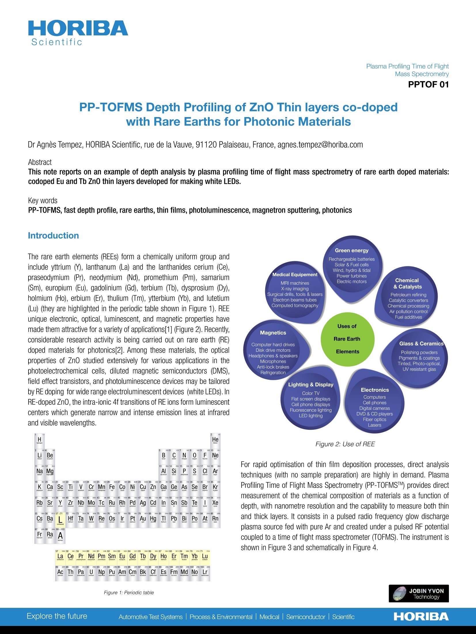
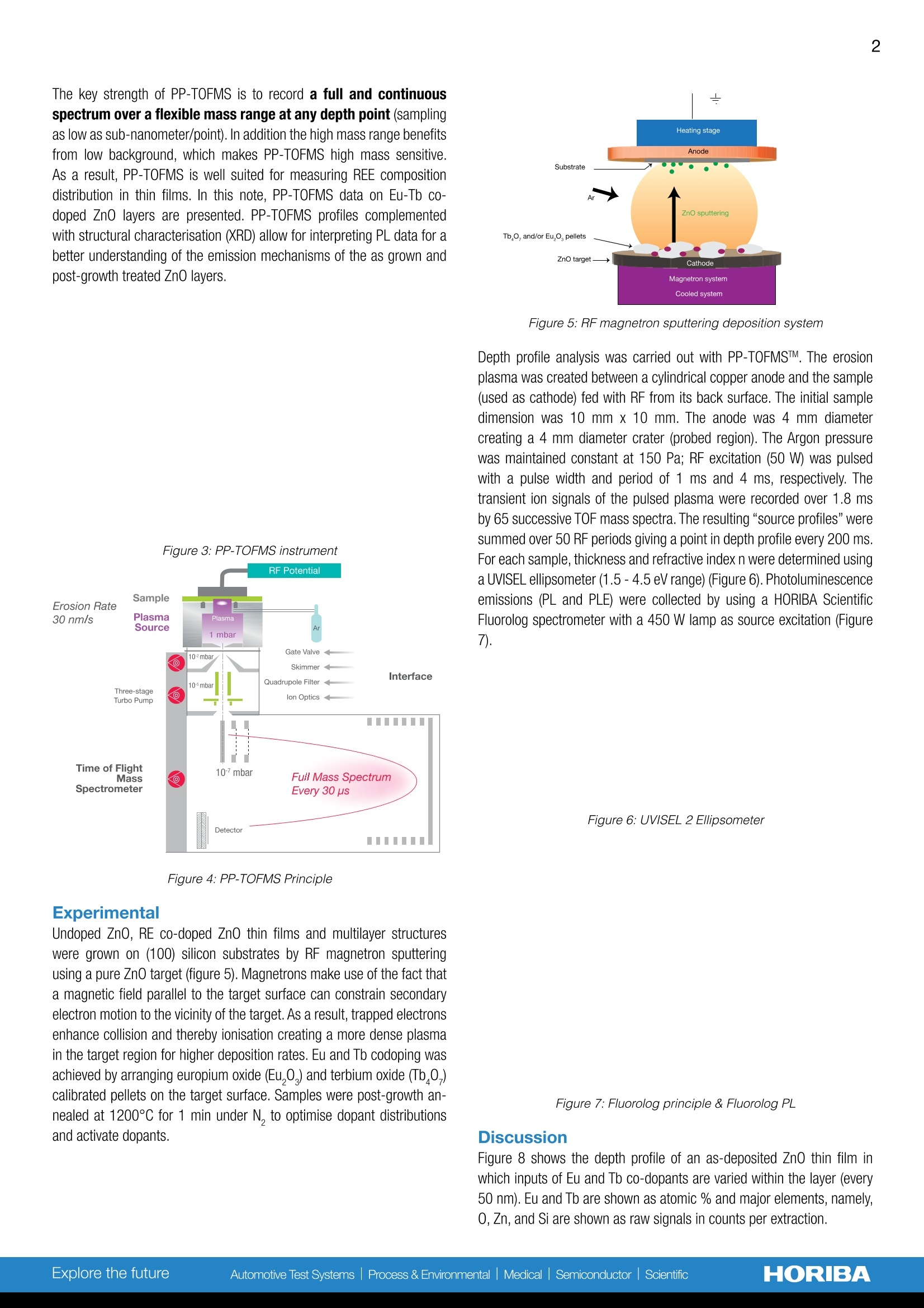
HORIBAScientific Material Sciences aopllcation Note Plasma Profiling Time of FlightMass Spectrometry PPTOF 01 PP-TOFMS Depth Profiling of ZnO Thin layers co-dopedwith Rare Earths for Photonic Materials Dr Agnes Tempez, HORIBA Scientific, rue de la Vauve, 91120 Palaiseau, France,agnes.tempez@horiba.com Abstract This note reports on an example of depth analysis by plasma profiling time of flight mass spectrometry of rare earth doped materials:codoped Eu and Tb Zn0 thin layers developed for making white LEDs. Key words PP-TOFMS, fast depth profile, rare earths, thin films, photoluminescence, magnetron sputtering, photonics The rare earth elements (REEs) form a chemically uniform group andinclude yttrium (Y), lanthanum (La) and the lanthanides cerium (Ce),praseodymium (Pr), neodymium (Nd), promethium (Pm), samarium(Sm), europium (Eu), gadolinium (Gd), terbium (Tb), dysprosium (Dy),holmium (Ho), erbium (Er), thulium (Tm), ytterbium (Yb), and lutetium(Lu) (they are highlighted in the periodic table shown in Figure 1). REEunique electronic, optical, luminescent, and magnetic properties havemade them attractive for a variety of applications[1] (Figure 2). Recently,considerable research activity is being carried out on rare earth (RE)doped materials for photonics[2]. Among these materials, the opticalproperties of ZnO studied extensively for various applications in thephotoelectrochemical cells, diluted magnetic semiconductors (DMS),field effect transistors, and photoluminescence devices may be tailoredby RE doping for wide range electroluminescent devices (white LEDs). InRE-doped Zn0, the intra-ionic 4f transitions of RE ions form luminescentcenters which generate narrow and intense emission lines at infraredand visible wavelengths. LaCePrNdPmSmEuGdTbDyHoEr TmYbLuAcThPaUNpPuAmCmBkCfEsFmMdNo Figure 2: Use of REE For rapid optimisation of thin film deposition processes, direct analysistechniques (with no sample preparation) are highly in demand. PlasmaProfiling Time of Flight Mass Spectrometry (PP-TOFMSTM) provides directmeasurement of the chemical composition of materials as a function ofdepth, with nanometre resolution and the capability to measure both thinand thick layers. It consists in a pulsed radio frequency glow dischargeplasma source fed with pure Ar and created under a pulsed RF potentialcoupled to a time of flight mass spectrometer (TOFMS). The instrument isshown in Figure 3 and schematically in Figure 4. The key strength of PP-TOFMS is to record a full and continuousspectrum over a flexible mass range at any depth point (samplingas low as sub-nanometer/point). In addition the high mass range benefitsfrom low background, which makes PP-TOFMS high mass sensitive.As a result, PP-TOFMS is well suited for measuring REE compositiondistribution in thin films. In this note, PP-TOFMS data on Eu-Tb co-doped ZnO layers are presented. PP-TOFMS profiles complementedwith structural characterisation (XRD) allow for interpreting PL data for abetter understanding of the emission mechanisms of the as grown andpost-growth treated Zn0 layers. Figure 3: PP-TOFMS instrument Figure 4: PP-TOFMS Principle Experimental Undoped ZnO, RE co-doped ZnO thin films and multilayer structureswere grown on (100) silicon substrates by RF magnetron sputteringusing a pure Zn0 target (figure 5). Magnetrons make use of the fact thata magnetic field parallel to the target surface can constrain secondaryelectron motion to the vicinity of the target. As a result, trapped electronsenhance collision and thereby ionisation creating a more dense plasmain the target region for higher deposition rates. Eu and Tb codoping wasachieved by arranging europium oxide (Eu,0.) and terbium oxide (Tb0,)calibrated pellets on the target surface. Samples were post-growth an-nealed at 1200℃ for 1 min under N, to optimise dopant distributionsand activate dopants. Figure 5: RF magnetron sputtering deposition system Depth profile analysis was carried out with PP-TOFMSTM. The erosionplasma was created between a cylindrical copper anode and the sample(used as cathode) fed with RF from its back surface. The initial sampledimension was 10 mm x 10 mm. The anode was 4 mm diametercreating a 4 mm diameter crater (probed region). The Argon pressurewas maintained constant at 150 Pa; RF excitation (50 W) was pulsedwith a pulse width and period of 1 ms and 4 ms, respectively. Thetransient ion signals of the pulsed plasma were recorded over 1.8 msby 65 successive TOF mass spectra. The resulting “source profiles" weresummed over 50 RF periods giving a point in depth profile every 200 ms.For each sample, thickness and refractive index n were determined usinga UVISEL ellipsometer (1.5-4.5 eV range) (Figure 6). Photoluminescenceemissions (PL and PLE) were collected by using a HORIBA ScientificFluorolog spectrometer with a 450 W lamp as source excitation (Figure7). Figure 6: UVISEL 2 Ellipsometer Figure 7: Fluorolog principle & Fluorolog PL Discussion Figure 8 shows the depth profile of an as-deposited ZnO thin film inwhich inputs of Eu and Tb co-dopants are varied within the layer (every50 nm). Eu and Tb are shown as atomic % and major elements, namely,0, Zn, and Si are shown as raw signals in counts per extraction. We have used the thickness determined by ellipsometry to convert theraw PP-TOFMS measurement time (X axis) to depth (in nm). Tb and Euconcentrations are obtained by simple calculation of ion beam ratio*without any calibration. IBR is the ratio between signal of a peakcorrected for isotopic abundance of corresponding isotope and the sumof ion matrix signals corrected for isotopic abundance. Here, 30Si, 67Zn,and 160 are used as matrix ions . It is important to note that this profilewas obtained in less than 1 min. Figure 8:ZnO thin film depth profile In this study, photoluminescence signal was detected on annealedsamples whereas as-deposited samples were non-active (Figure 9). Asshown in Figure 10 PP-TOFMS depth profiles of both as-deposited andannealed samples evidence the high Si diffusion in Zn upon annealingand formation of a new matrix. This study extends to several doped andundoped ZnO thin layers. More details may be found in reference [3]. Figure 9: Photoluminescence of ZnO layer Figure 10: Depth profiles of as-deposited & annealed samples The high PP-TOFMS sensitivity in rare earth elements is explained bythe unique TOFMS capability of recording a complete mass spectrumevery 30 ps and the ultra-low background for high mass elements. Thisis illustrated by the full mass spectrum taken from a single point of thedepth profile (i.e. integrated over a 0.3 nm depth) shown in both linearand semi logarithmic scales in Figures 11 and 12. Below mass 50, ionssuch as C, 0,OH,CO,... are present. Figure 11: Mass elements spectrum (linear scale) Figure 12: Mass elements spectrum (logarithmic scale) The acquisition of a continuous full spectrum gives access to signals ofall isotopes. The spectrum in Figure 13 zoomed on the two Europiumisotopes shows perfect fit between 151Eu and 153Eu signals (violet line) andthe natural isotopic distribution (green line) of Europium. Such isotopicabundance matching is readily checked with PP-TOFMS software andallows for picking non-interfered isotope. Figure 13: Europium isotopes Conclusions This example shows that PP-TOFMS is a fast and reliable techniquefor depth profiling of rare earth doped Zn0 thin films. Tb and Euprofiles are obtained with high sensitivity and high depth resolution. Thistype of information is typically provided by SIMS, RBS or depthprofiling XPS but not as rapidly and readily and at a higher cost.Such profiles turn out to be powerful complementary information to un-derstand photoluminescence data. This example extends to similar materials for photonics (lighting,display,solar energy industries) applications such as other wide bandgap semi-conductors (SiC,GaN...), nitrides and oxynitrides layers, silicon nano-ob-jects, glasses... doped with Yb,Y, Sm, Er, Nd, Pr, and Tm... Definition of lon Beam Ratio or IBR N: Number of all elements (ion peaks being investigated) N: Number of main elements included in a matrix I:Signal of an isotope i of an element j Al:Abundance of an isotope i of an elementj X: An element of interest References [1] The Rare Earth Elements: Fundamentals and Applications, David A.Atwood, John Wiley & Sons, 2013. [2] Andries Maijerink, Lanthanide lons as Photon Managers for Solar Cells,Material Matters, 6 (4) 113 (2011). [3] A. Ziani, A. Tempez, C. Frilay, C. Davesnne, C. Labbe, Ph. Marie, S.Legendre and X. Portier, Concentration determination and activation ofrare earth dopants in zinc oxide thin films, EMRS Fall 2013 Proceedings,physica status solidi All materials containing rare earth elements: nanometer thick thin films atlevel down to 101 atom/cm3 and atomic ppb level in thicker films or bulkmaterials. Examples: GaN,SiC, glass, hard coating, steels... Check on other HORIBA techniques in this fieldStructural properties: Raman Spectroscopy Thickness and optical properties: Spectroscopic EllipsometryPurity determination: ICP-0ES Defect studies: Cathodoluminescence Acknowledgments C. Frilay, A. Ziani, and F. Gourbilleau from the Research Center for lons,Materials and Photonics (CIMAP, University of Caen, France) are kindlythanked for allowing the use of results on Zn0 samples. JOBIN YVON Technology info.sci@horiba.com www.horiba.com/scientific France:+33 (0)1 69 747200 Germany: +49 (0)89 4623 17-0Italy: +39 2 57603050 Japan:Brazil:: +55 (0)112923 5400 Other: +81 (0)3 6206 4721 JOBIN YVONTechnologyHORIBAExplore the futureAutomotive Test SystemsslProcess &EnvironmentalMedicalISemiconductorScientific
关闭-
1/4
-
2/4
还剩2页未读,是否继续阅读?
继续免费阅读全文产品配置单
HORIBA(中国)为您提供《掺杂有稀土元素的氧化锌薄膜分析》,该方案主要用于其他中null检测,参考标准《暂无》,《掺杂有稀土元素的氧化锌薄膜分析》用到的仪器有null。
我要纠错
相关方案
 咨询
咨询