方案详情文
智能文字提取功能测试中
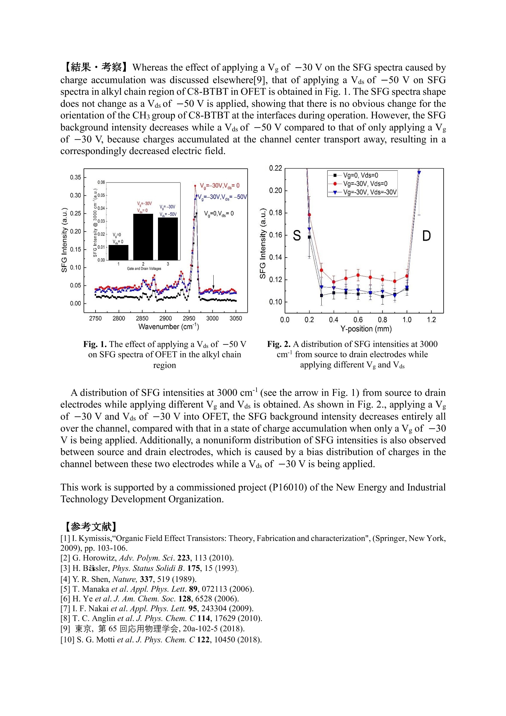
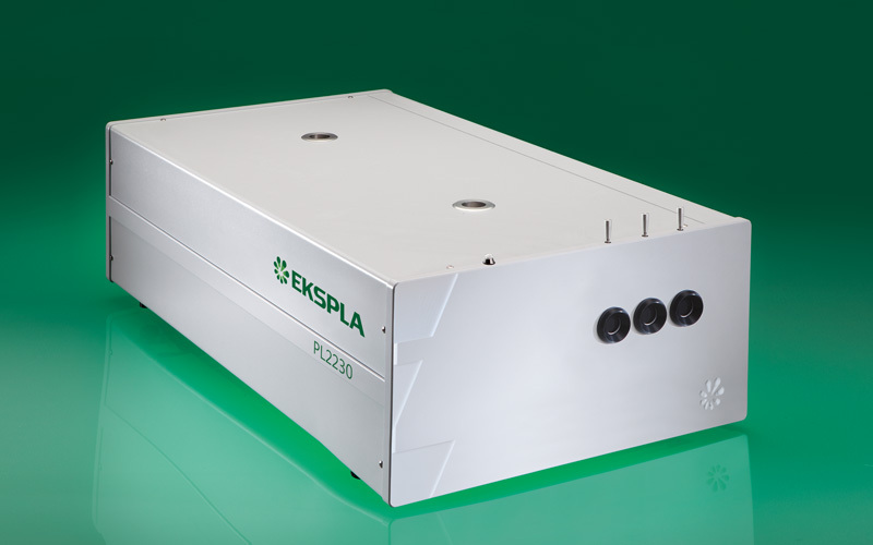
3P049 Visualization of charge activities at the semiconductor/insulator interface ofOFET during operation by SFG spectroscopy oHaiya Yang, Masato Miyashita, and Takayuki Miyamae Nanomaterials Research Institute, National Institute of Advanced Industrial Science and Technology (AIST), Japan "Research Association ofHigh-Throughput Design and Development for AdvancedFunctional Materials (ADMAT), Japan Abstract】 In our work, being aimed at clarifying the mechanism of charge transport inorganic field-effect transistors (OFET) during operation and furthermore designing new OFETwith higher performances, interfaces of OFET are studied by sum-frequency generation (SFG)spectroscopy. The effect of drain voltage on SFG spectra ofOFET is obtained. A biasdistribution of SFG intensities at 3000 cmbetween source and drain electrodes caused bycharge transport is obtained. Charge activities at the semiconductor/insulator interface ofOFETduring operation are preliminary mapped by SFG spectroscopy. 【序】 OFET have developed a lot since 30 years ago for their industrial applications such asdisplays and mechanical sensors[1].Studying interfaces ofOFET where charge transport occuris a motivating topic for good device performance[2]. Although theoretical simulation can beused to elucidate charge transfer at interfaces of OFET[3], it is problematic to experimentallyobserve it for lacking of a highly surface-selective analytical method. Second harmonicgeneration (SHG) and SFG, as inherently surface-selective methods[4], have been utilized intostudying interfaces of OFET since 2006 while electric-field was induced[5-10]. Among thesework, visualization of charge accumulation in OFET is rarely intriguing because it provides atwo-dimensional XY-map and thus a complete image of charge activities in the conductingchannel of OFET[7, 9]. However, charge transport at interfaces of OFET that essentiallydetermines the device performance has not been visualized. In this work, by using SFGspectroscopy with stepping motors installed, we obtained the effect of drain voltage on SFGspectra of OFET, a bias distribution of SFG intensities at 3000 cmfrom source to drainelectrodes, and a 4.0×4.0 mm XY-map of charge activities at the semiconductor/insulatorinterface of OFET during operation. 【方法(実験·理論)】】 A top-contact bottom-gate OFET was constructed with two goldelectrodes of 30nmthick.1a50-nm-thicklayer of 2,7-dioctyl[1]benzothieno[3,2-b]benzothiophene (C8-BTBT), and a silicon substrate with a 200-nm-thick layer of SiO2 coatedabove as the gate dielectric. The length/width for a channel is 1000/1000 um. An SFGspectrometer is consisted of a picosecond laser (Ekspla,PL2231-50) of 50 Hz repetition rate, aharmonic unit (Ekspla, SFGH500-2H), and an optical parametric generation unit (Ekspla,PG501-DFG1P). The output energies oflasers were controlled at the minimum conditions toavoid sample damage. The polarizations were set in PPP during measurements. The incidentangles for visible and infrared beams were 65°and 55°, respectively. The SFG spectra weremeasured at the channel center. A precision source/measure unit (Keysight, B2902A) wasinduced to the SFG spectrometer to apply gate and drain voltages into OFET. The scanningsteps were 0.1 mm for the distribution of SFG intensities and 0.2 mm for the XY-map. Theplane of visible, infrared and SFG beams is parallel to that of source and drain in the SFGspectra measurements but perpendicular in the distribution of SFG intensities and the XY-mapmeasurements. The resolutions in X and Y directions are 0.2 mm and 0.1 mm, respectively. 【結果·考察】 Whereas the effect of applying a Vg of -30 V on the SFG spectra caused bycharge accumulation was discussed elsewhere[9], that of applying a Vds of -50 V on SFGspectra in alkyl chain region of C8-BTBT in OFET is obtained in Fig. 1. The SFG spectra shapedoes not change as a Vds of -50 V is applied,showing that there is no obvious change for theorientation of the CH3 group ofC8-BTBT at the interfaces during operation. However, the SFGbackground intensity decreases while a Vas of-50 V compared to that of only applying a Vgof -30 V, because charges accumulated at the channel center transport away, resulting in acorrespondingly decreased electric field. Fig. 1. The effect of applying a Vds of -50 Von SFG spectra ofOFET in the alkyl chainregion Fig. 2. A distribution of SFG intensities at 3000cmfrom source to drain electrodes whileapplying different Vg and Vds A distribution of SFG intensities at 3000 cm(see the arrow in Fig. 1) from source to drainelectrodes while applying different Vg and Vds is obtained. As shown in Fig. 2.,applying a Vgof -30 V and Vds of -30 Vinto OFET, the SFG background intensity decreases entirely allover the channel, compared with that in a state of charge accumulation when only a Vg of -30V is being applied. Additionally, a nonuniform distribution of SFG intensities is also observedbetween source and drain electrodes, which is caused by a bias distribution of charges in thechannel between these two electrodes while a Vds of -30 V is being applied. This work is supported by a commissioned project (P16010) of the New Energy and IndustrialTechnology Development Organization. ( 【参考文献】 ) [1]I. Kymissis,"Organic Field Effect Transistors: Theory, Fabrication and characterization", (Springer, New York,2009), pp. 103-106. ( [2] G. Horowitz, Adv. Polym. Sci. 223,11 3 (2010). ) ( [3] H. Bassler, Phys. S tatus Solidi B. 175, 15(1993). ) ( [4] Y. R. Shen, Nature, 337, 519 (1989). ) ( [5] T. Manaka et al. Appl. Phys. Lett . 89,072113 (2006). ) ( [6] H. Ye et al. J. Am . Chem. Soc. 128,6528 ( 2006). ) ( [7]I. F. Nakai et al. Appl. Phys. Lett. 95,243304(2009). ) ( [8]T. C. Anglin et al. J. Phys. Chem. C 114 , 17629(2010). ) ( [9 ] 東京,第65回应用物理学会,20a-102-5(2018). ) ( [10] S. G. Motti et al. J . Phys . Chem. C 1 22, 1 0450 ( 2 018). ) In our work, being aimed at clarifying the mechanism of charge transport in organic field-effect transistors (OFET) during operation and furthermore designing new OFET with higher performances, interfaces of OFET are studied by sum-frequency generation (SFG) spectroscopy. The effect of drain voltage on SFG spectra of OFET is obtained. A bias distribution of SFG intensities at 3000 cm-1 between source and drain electrodes caused by charge transport is obtained. Charge activities at the semiconductor/insulator interface of OFET during operation are preliminary mapped by SFG spectroscopy.
关闭-
1/2

-
2/2
产品配置单
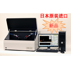
北京欧兰科技发展有限公司为您提供《OFET器件半导体/绝缘体界面中和频光谱测量检测方案(其它光谱仪)》,该方案主要用于其他中和频光谱测量检测,参考标准《暂无》,《OFET器件半导体/绝缘体界面中和频光谱测量检测方案(其它光谱仪)》用到的仪器有Ekspla SFG 表面和频光谱分析系统、Ekspla PL2230型高能量皮秒激光器。
我要纠错
推荐专场
相关方案






 咨询
咨询


