方案详情文
智能文字提取功能测试中
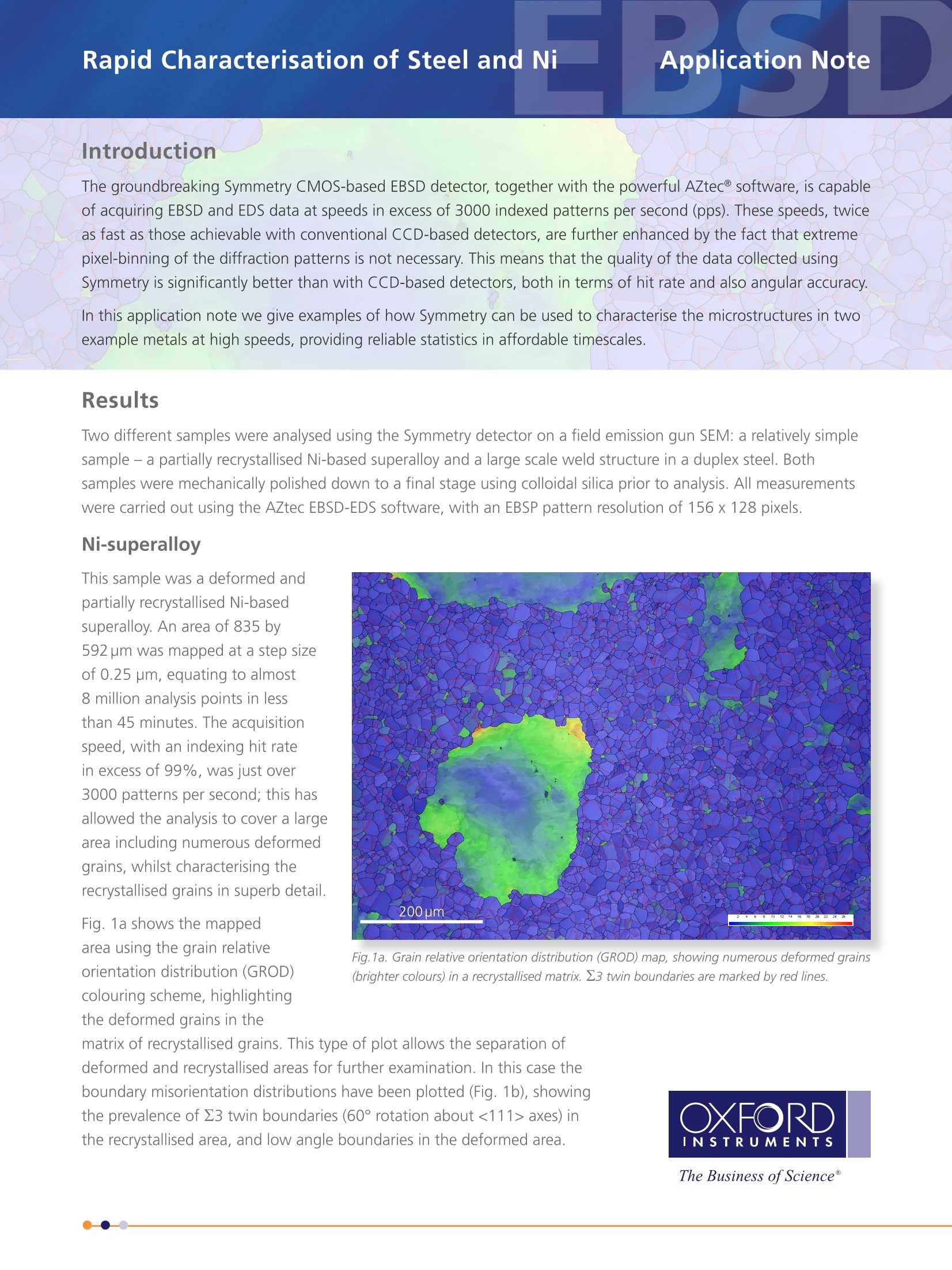
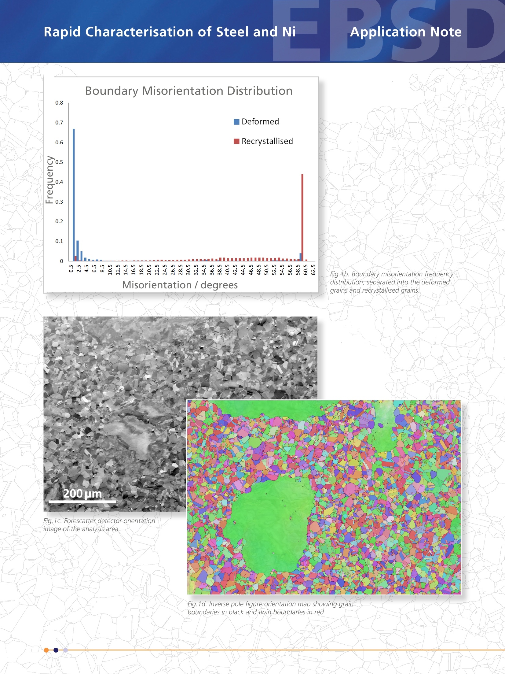
Rapid Characterisation of Steel and Ni Rapid Characterisation of Steel and Ni Application Note Introduction The groundbreaking Symmetry CMOS-based EBSD detector, together with the powerful AZtec@ software, is capableof acquiring EBSD and EDS data at speeds in excess of 3000 indexed patterns per second (pps). These speeds, twiceas fast as those achievable with conventional CCD-based detectors, are further enhanced by the fact that extremepixel-binning of the diffraction patterns is not necessary. This means that the quality of the data collected usingSymmetry is significantly better than with CCD-based detectors, both in terms of hit rate and also angular accuracy. In this application note we give examples of how Symmetry can be used to characterise the microstructures in twoexample metals at high speeds, providing reliable statistics in affordable timescales. Results Two different samples were analysed using the Symmetry detector on a field emission gun SEM: a relatively simplesample - a partially recrystallised Ni-based superalloy and a large scale weld structure in a duplex steel. Bothsamples were mechanically polished down to a final stage using colloidal silica prior to analysis. All measurementswere carried out using the AZtec EBSD-EDS software, with an EBSP pattern resolution of 156 x 128 pixels. This sample was a deformed andpartially recrystallised Ni-basedsuperalloy. An area of 835 by592 pm was mapped at a step sizeof 0.25 um, equating to almost8 million analysis points in lessthan 45 minutes. The acquisitionspeed, with an indexing hit ratein excess of 99%, was just over3000 patterns per second; this hasallowed the analysis to cover a largearea including numerous deformedgrains, whilst characterising therecrystallised grains in superb detail. Fig. 1a shows the mappedarea using the grain relativeorientation distribution (GROD)colouring scheme, highlightingthe deformed grains in the Fig.1a. Grain relative orientation distribution (GROD) map, showing numerous deformed grains(brighter colours) in a recrystallised matrix. 23 twin boundaries are marked by red lines. matrix of recrystallised grains. This type of plot allows the separation ofdeformed and recrystallised areas for further examination. In this case theboundary misorientation distributions have been plotted (Fig. 1b), showingthe prevalence of 23 twin boundaries (60°rotation about <111> axes) inthe recrystallised area, and low angle boundaries in the deformed area. The Business ofScience@ Application Note Fig.1b. Boundary misorientation frequencydistribution, separated into the deformedgrains and recrystallised grains. 200um Fig.1c. Forescatter detector orientationimage of the analysisarea Fig. 1d. Inverse pole figure orientation map showing grain boundaries in black and twin boundaries in red Weld In this example, a welded sample of duplex stainless steel was examined using Large Area Mapping. The challengewas to examine a wide transect (~ 5 mm across) yet to retain sufficient resolution to measure accurately the smallgrains in both the weld itself and the base metal. The area was mapped with a 0.25 pm step size, at ~2000 indexedpatterns per second. In total 96 maps were collected, totalling more than 45 million points with a 98.5% hit rate.The resulting phase map (Fig. 2a) shows clearly the variation from the base metal on the right to the fusion zoneon the left. This large area, high resolution scan allows a detailed study of the textures, grain sizes and phasedistributions across the different zones of the weld. Despite the obvious change in the microstructure, there is little change in the phase fraction between the basemetal and the fusion zone (a ferrite to austenite ratio of 55:45 compared to 54:46 respectively). However, in theheat affected zone (HAZ), the phase fractions change significantly to 71% ferrite and 29% austenite. Although the fusion zone appears to be significantly coarser grained, the full scale images shown in Figs. 2b and 2cshow the presence of many very small austenite grains, <5 um diameter. These reduce the mean grain size of theaustenite in the fusion zone to only 6.3 um, significantly less than the 9.5 um mean in the base metal (both figuresbased on more than 20,000 grains). The large area analysis also enables a statistically valid study of the variation in texture across this weld margin. Thecontoured pole figures in Fig. 2d and 2e show the change in texture in the ferrite between the base metal and thefusion zone. Within the base metal there is a fairly strong alignment of {100} poles normal to the rolling direction,but little clear texture is present in the fusion zone, with the higher densities resulting from a few very large grains. Fig. 2a. Phase map across the weld margin in a duplex steel. Red- ferrite, blue -austenite. The fusion zone (weld) is tothe left of the map, the base metal to the right. The yellow box marks the area highlighted on the next page.... Fig. 2b. Phase map of the area marked in (a) in higher detail.Red-ferrite, blue -austenite. Fig. 2d. Contoured pole figures ({100}, {110} and {111}) for ferritewithin the fusion zone. Fig. 2c. Orientation map of the area marked in (a) in higher detail(inverse pole figure colour scheme, with grain boundaries in black). Fig. 2e. Contoured pole figures ({100}, {110} and {111}) for ferritewithin the base metal. Conclusion These two contrasting examples demonstrate how the AZtec EBSD software in combination with the SymmetryEBSD detector is an ideal combination for the rapid and effective characterisation of a range of metal and alloysamples. In single phase metal samples, indexing speeds in excess of 3000 pps are achieved with no compromise ondata quality or indexing hit rate, whereas in dual-phase materials speeds in excess of 2000 pps are commonplace.These speeds are achieved without extraordinary beam currents: typically ~10 nA is sufficient to achieve excellentpattern quality and indexing at 3000 pps. These high speeds and associated, uncompromised data quality makes Symmetry an extremely powerful EBSDdetector for grain size, texture and phase characterisation of all but the most complex samples. What took hoursor even days with conventional CCD-based detectors can now be completed in a matter of minutes, expanding theappeal of EBSD as a routine characterisation tool. www.oxford-instruments.com/symmetry IntroductionThe groundbreaking Symmetry CMOS-based EBSD detector, together with the powerful AZtec® software, is capableof acquiring EBSD and EDS data at speeds in excess of 3000 indexed patterns per second (pps). These speeds, twiceas fast as those achievable with conventional CCD-based detectors, are further enhanced by the fact that extremepixel-binning of the diffraction patterns is not necessary. This means that the quality of the data collected usingSymmetry is significantly better than with CCD-based detectors, both in terms of hit rate and also angular accuracy.In this application note we give examples of how Symmetry can be used to characterise the microstructures in twoexample metals at high speeds, providing reliable statistics in affordable timescales.
关闭-
1/4
-
2/4
还剩2页未读,是否继续阅读?
继续免费阅读全文产品配置单
牛津仪器科技(上海)有限公司为您提供《金属及合金中表征检测方案(EBSD系统)》,该方案主要用于合金中理化分析检测,参考标准《暂无》,《金属及合金中表征检测方案(EBSD系统)》用到的仪器有EBSD探测器Symmetry S3 牛津仪器。
我要纠错
推荐专场
电子背散射衍射系统(EBSD)
更多
相关方案
 咨询
咨询