产品介绍
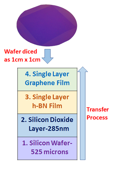
CVD Graphene/CVD Hexagonal Boron Nitride heterostructure on SiO2/Si wafer
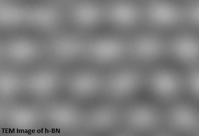
Properties of Graphene/h-BN Film:
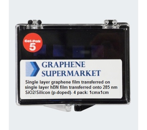
Single Layer Graphene Film on Single Layer h-BN Film transferred onto 285 nm (p-doped) SiO2/Si wafer
Size: 1cmx1cm; 4 pack
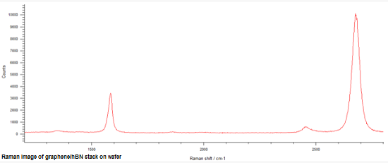
The thickness and quality of each film is controlled by Raman Spectroscopy
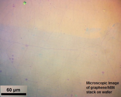
The coverage of this product is about 98%
The films are continuous, with minor holes and organic residues
High Crystalline Quality
The graphene film is premodominantly single layer (more than 95%) with occasional small multilayer islands (less than 5% bi-layers)
Sheet Resistance: 430-800 Ω/square
Properties of Silicon/Silicon Dioxide Wafers:
Oxide Thickness: 285 nm
Oxide Thickness: 285 nm
Color: Violet
Wafer thickness: 525 micron
Resistivity: 0.001-0.005 ohm-cm
Type/Dopant: P/Boron
Orientation: <100>
Front Surface: Polished
Back Surface: Etched
供应商
-

银牌会员 第12年
- 推荐专场
- 同类产品
- 该厂商产品
- 相关厂商
- 赛多利斯酸度计PB-10
- 赛多利斯水分测定仪MA35M-1CN
- 赛多利斯Charging Stand充电支架[REF 730981]
- 石油温度计
- Ceramus® 全能型瓶口分配器分液器
- DS-360-36石墨消解仪
- EM 有机型瓶口分配器分液器移液器
- 采样钢瓶金属软管
- 迪马科技塑化剂(邻苯二甲酸酯、双酚A)单标及混标
- 非洛地平四边篮(缓释片专用)
- 食品安全石墨消解仪 土壤环境石墨消解仪
- 实验室智能石墨消解仪 多孔批量处理加热均匀
- 溶出度仪DV系列高容量取样针
- 溶出度仪沉降篮
- 溶出度仪沉降篮安装拆卸专用工具
- 溶出度仪沉降篮篮轴
- 溶出度仪沉降篮篮轴(DISTEK专用)
- 溶出度仪沉降篮篮轴(ERWEKA专用)
- 溶出度仪沉降篮篮轴(SOTAX专用)
- 溶出度仪沉降篮篮轴(安捷伦Agilent专用)
- 溶出度仪沉降篮篮轴储存器
- 溶出度仪沉降篮篮子储存器
- 溶出度仪沉降装置
- 溶出度仪沉降装置用316不锈钢丝
- 纳谱分析 ChromCore C18-MS Pesticides中药农残专用柱 C18(ODS)柱
- 纳谱分析 EcoPak 120 C18色谱柱(ODS)柱 EcoPak 120 C18 Plus色谱柱
- 纳谱分析 BioCore SEC-300色谱柱 水溶性SEC柱
- 纳谱分析 SelectCore HLB-A 中药农药专用固相萃取柱
- Shim-pack GISS C18(ODS)柱
- Shim-pack VP-ODS C18液相色谱柱
- 岛津 Shim-pack GISS C18(ODS)柱
- 岛津 Shim-pack GIS C18(ODS)柱
- 岛津 Shim-pack GIS系列 Shim-pack GIS C18-P 液相色谱柱C18(ODS)柱
- 岛津 Shim-pack GIST系列 Shim-pack GIST C18-AQ 液相色谱柱
- 北京德泉兴业商贸有限公司
- 图拉扬科技有限公司
- 博医康 (北 京)仪器有限公司
- 乐枫生物
- 济南弗莱德科技有限公司
- 上海左乐仪器有限公司
- 北京中科奥博科技有限公司
- 北京冠远科技有限公司
- 北京嘉德利达科技有限公司
- 保定至方泵业有限公司
- 厦门隆力德环境技术开发有限公司
- 顶尖科仪(中国)股份有限公司
- 浚和(上海)仪器科技有限公司
- 滨松光子学商贸(中国)有限公司
- 洛科仪器股份有限公司
- 成贯仪器(上海)有限公司
- 上海新拓分析仪器科技有限公司
- 上海尖丰光电技术有限公司
- 海德创业(北京)生物科技有限公司
- 上海达燊实业有限公司
- 北京博赛德科技有限公司
- 海洋光学亚洲公司
- 上海默西科学仪器有限公司
- 威立雅水处理技术(上海)有限公司