产品介绍
Substrate:
Sapphire (c-cut)
Quartz (Silica)
TEM grids (please supply grids)
Thermal Oxide (SiO2/Si)
Polyethylene terephthalate – PET Substrates
Pick your own substrates (please define the substrate type)
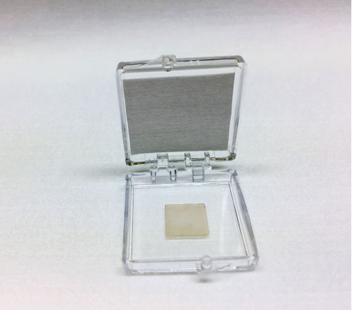
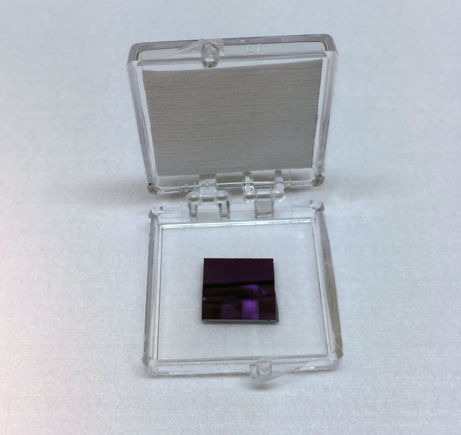
Our R&D has developed scalable methods to transfer large area h-BN, graphene, MoS2, MoSe2, WS2, WSe2, ReS2, ReSe2, SnS2, SnSe2, PtS2, and PtSe2 sheets onto almost any substrates (please see Question 3 below). Our team uses extremely delicate steps and processes to keep the 2D layers clean and unaltered. Our processes are carried out under ultra-high purity environment so that the material quality is not sacrificed. However, because of the custom nature of the production process, all transferred CVD sales are final and non-refundable.
During the online check-out or when requesting a formal quote, please indicate desired substrate, desired CVD material (see list of CVD products here), and any additional requirements / suggestions.
Frequently asked questions
Q1: Can you transfer monolayers onto TEM grids?
A: Yes, we can transfer any CVD product onto any TEM grids. Our company requires you to select your own TEM grids, inform us the model, and send (extra) TEM grids so that we can do tests to deliver you good quality samples.
Q2: Can you guarantee that CVD monolayers will be same quality after the transfer?
A: Transfer process requires polymeric stamping and / or chemical processes. These steps generally will introduce some cracks and voids in the samples. But if you selected to transfer full area CVD monolayers, they will still be at large scales. There might be some folding, wrinkling effects, and this is normal. If your CVD monolayer is luminescent, after the transfer optical properties will remain similar with PL emission at the same wavelenghts
Q3: What kind of substrates can you transfer onto?
A: You would be surprised to know but we have transferred CVD monolayers more than 100 different substrates to date. Examples include, Bragg reflectors, plasmonic structures, SiO2/Si, sapphire, quartz, mica, PET, polymer, other 2D materials, glass, TEM grids, metals, and even on a diamond!
Q4: What is the typical processing times?
A: This will depend on your project, chemistry required, and your sets of requirements towards sample production. It is typically around 1-3 weeks.

供应商
-

银牌会员 第13年
- 推荐专场
- 同类产品
- 相关厂商
- 赛多利斯酸度计PB-10
- 赛多利斯水分测定仪MA35M-1CN
- 赛多利斯Charging Stand充电支架[REF 730981]
- 石油温度计
- Ceramus® 全能型瓶口分配器分液器
- DS-360-36石墨消解仪
- EM 有机型瓶口分配器分液器移液器
- 采样钢瓶金属软管
- 迪马科技塑化剂(邻苯二甲酸酯、双酚A)单标及混标
- 非洛地平四边篮(缓释片专用)
- 食品安全石墨消解仪 土壤环境石墨消解仪
- 实验室智能石墨消解仪 多孔批量处理加热均匀
- 溶出度仪DV系列高容量取样针
- 溶出度仪沉降篮
- 溶出度仪沉降篮安装拆卸专用工具
- 溶出度仪沉降篮篮轴
- 溶出度仪沉降篮篮轴(DISTEK专用)
- 溶出度仪沉降篮篮轴(ERWEKA专用)
- 溶出度仪沉降篮篮轴(SOTAX专用)
- 溶出度仪沉降篮篮轴(安捷伦Agilent专用)
- 溶出度仪沉降篮篮轴储存器
- 溶出度仪沉降篮篮子储存器
- 溶出度仪沉降装置
- 溶出度仪沉降装置用316不锈钢丝
- 北京华盛谱信仪器有限责任公司
- 广州格丹纳仪器有限公司
- 北京中仪宇盛科技有限公司
- 博医康 (北 京)仪器有限公司
- 北京艾若泰克科技有限公司
- 上海莘浦科技有限公司
- 成贯仪器(上海)有限公司
- 中科瑞捷(天津)科技有限公司
- 北京共赢联盟国际科技有限公司
- 济南弗莱德科技有限公司
- 滨松光子学商贸(中国)有限公司
- 成器智造(北京)科技有限公司
- 深圳冠亚水分仪科技
- 北京天翔飞域科技有限公司
- 国力天(深圳)科技有限公司
- 北京钮因华信科技发展有限公司
- 顶尖科仪(中国)股份有限公司
- 上海喆图科学仪器有限公司
- 图拉扬科技有限公司
- KPM分析集团
- 上海畅仪科学仪器有限公司
- 北京亚科晨旭科技有限公司
- 广东正业科技股份有限公司
- 浙江华琮仪器有限公司