方案摘要
方案下载| 应用领域 | 半导体 |
| 检测样本 | 光电器件 |
| 检测项目 | |
| 参考标准 | 无 |
The emergence of new materials have paved the way to nano-electronic and optoelectronic devices with improved or new capabilities. For instance, III-V based alloys have revolutionized the LED industry finding applications in high power electronics, and may speed up micro- electronic devices in the near future. Unfortunately, their wide scaled implementation is still limited by the presence of highly concentrated crystallographic or impurity defects. Such defects are typically of sub-nanometric size and are therefore difficult to observe directly. Defect metrology is by consequence of very high importance to assess fabrication processes. Three methods are traditionally implemented to determine the density of defects in optoelectronic devices
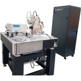
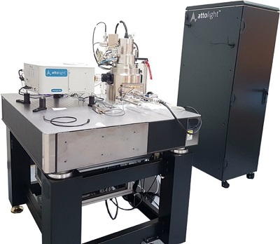
阴极荧光分析系统SEM-CL在光电材料的缺陷检测和计量方面的应用
文献贡献者


分子相互作用相互仪(MP-SPR)在小分子药物与人血清白蛋白的相互作用方面的应用
分子相互作用仪(MP-SPR)在活细胞中小化合物对G蛋白偶联受体(GPCR)刺激分析中的应用
分子相互作用相互仪(MP-SPR)在奶粉细菌检测方面的应用
相关产品
铝离子检测仪 MIPS
氟离子检测仪 MIPS
内毒素检测仪 MIPS
农药检测仪 MIPS
石英晶体微天平 MIPS
纳米等离子体传感分析仪 S2
纳米等离子体传感分析仪 M8
全晶圆工业阴极荧光CL-SEM系统 Santis 300
皮秒时间分辨阴极荧光 CL-SEM系统 Chronos
磁场成像显微镜系统 Magma EFI HiRes
磁场成像显微镜系统 Magma EFI
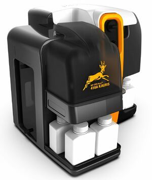
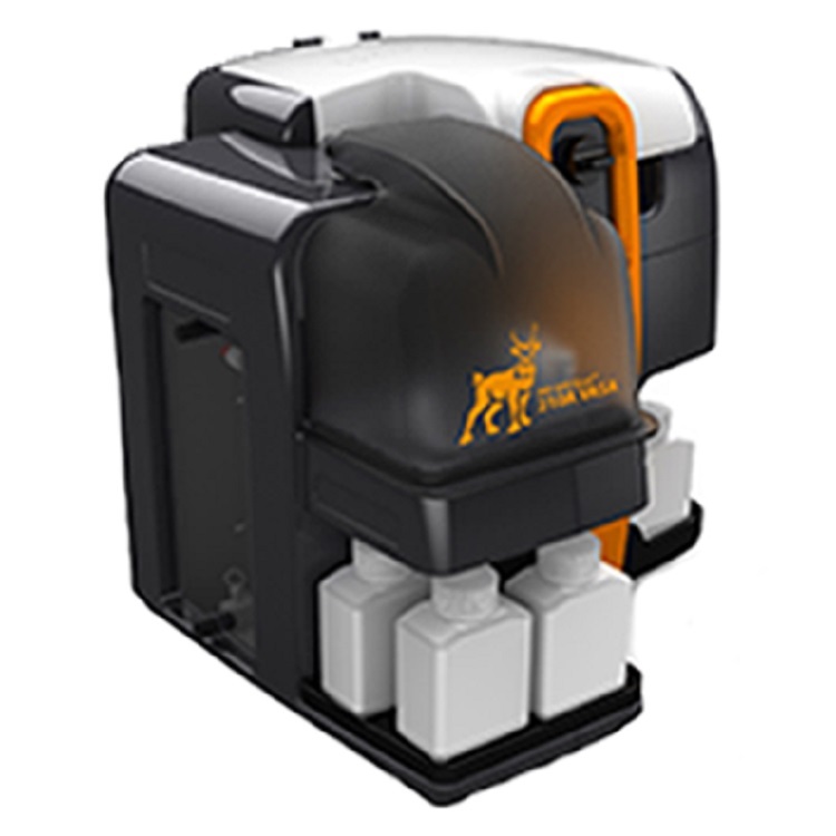
多参数表面等离子体共振分析仪(分子互作分析仪) MP-SPR 410A
离子辅助脉冲激光沉积系统 Ion-Assisted PLD System
大尺寸脉冲激光沉积系统 Large-Area PLD Systems
组合型脉冲激光沉积系统 Combinatorial PLD System

关注

拨打电话

留言咨询