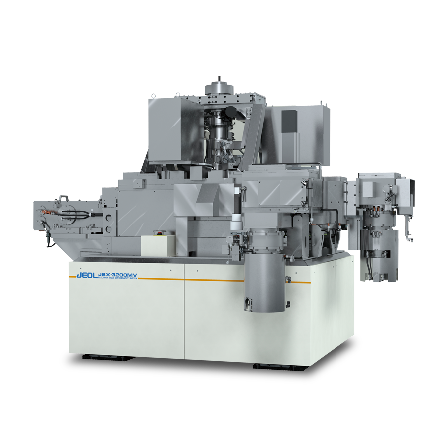
| 型号: | JBX-3200MV |
| 产地: | 日本 |
| 品牌: | 日本电子 |
| 评分: |
|


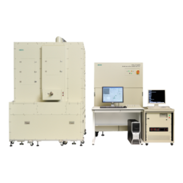
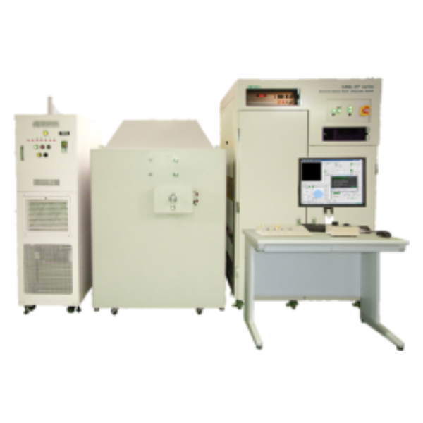
光刻机又名:掩模对准曝光机,曝光系统,光刻系统,紫外曝光机等;美国公司为全球领先的半导体设备供应商,多年来致力于掩模对准光刻机和匀胶机研发与生产,并且广泛应用于半导体、微电子、生物器件和纳米科技领域;该公司是目前世界上最早将光刻机商品化的公司之一,拥有雄厚的技术研发力量和设备生产能力;并且其设备被众多著名企业、研发中心、研究所和高校所采用;以优秀的技术、精湛的工艺和良好的服务,赢得了用户的青睐。
3D SEM image mosaics stitched over large areas and in 3D with CAD shape extraction
The CHIPSCANNER combines high-resolution electron optics, multiple high-efficiency electron detectors, and ultra-precise Laser Interferometer Stage technology with unique software to deliver homogenous large-area image mosaics for each layer with minimum stitching errors and stable brightness/contrast values and CAD shape extraction. With features such as
• Active focus control using laser height sensing
• Highest position and beam accuracy and stability, and
• A wide range of selectable electron detectors,
the CHIPSCANNER produces the most accurate large-area, high-resolution image mosaics directly acquired by an SEM instrument. Since the absolute position of each pixel, even over cm², is ultimately known to the accuracy provided by the laser interferometer stage and ultra-precise image calibrations, these images can be precisely stacked (3D-stitched).
Various high-speed detectors, flexible working distance, parallel detector stream handling and a high-speed scan generator allow precise and flexible image acquisition that is also high throughput.
Large-area, ultra-high-resolution 3D SEM imaging applications in chip reverse engineering, materials science, and life sciences (e.g. connectomics) require surfaces of up to cm² areas to be scanned with nm resolution and excellent layer to layer accuracy (‘3D stitching’) for layout and schematic extraction or 3D modeling. While traditional SEM instruments are inherently limited by small, uncalibrated fields of view (FOVs) and imprecise sample positioning, the CHIPSCANNER addresses these challenges by combining the resolution and flexibility of an SEM instrument with the accuracy, stability, and automation of an electron beam lithography (EBL) instrument – a core area of expertise at Raith. High-resolution, large-area image mosaics are created by capturing sequential SEM images and stitching them together for further analysis, while the laser interferometer stage and field-of-view calibration reduce overlap to an absolute minimum and thus reduce required computing. A true large-area 3D SEM!
相关产品

关注

拨打电话

留言咨询