方案详情文
智能文字提取功能测试中
View Article OnlineView Journal|View Issue View Article OnlineNanoscalePaper PAPER CrossMark< click for updates In situ formation and photo patterning of emissivequantum dots in small organic molecules Cite this: Nanoscale, 2015, 7, 11163 Ashu K. Bansal,Muhammad T. Sajjad, Francesco Antolini, Lenuta Stroea,Paulius Gecys, Gediminas Raciukaitis,.d Pascal Andre, Andreas Hirzer,Volker Schmidt, Luca Ortolani, Stefano Toffanin,9 Sybille Allard,Ullrich Scherfand Ifor D. W.Samuel*d Received 3rd March 2015,Accepted 15th May 2015 DOI: 10.1039/c5nr01401h www.rsc.org/nanoscale Nanostructured composites of inorganic and organic materials are attracting extensive interest for elec-tronic and optoelectronic device applications. Here we report a novel method for the fabrication and pat-terning of metal selenide nanoparticles in organic semiconductor films that is compatible with solutionprocessable large area device manufacturing. Our approach is based upon the controlled in situdecomposition of a cadmium selenide precursor complex in a film of the electron transporting material1,3,5-tris(N-phenyl-benzimidazol-2-yl)-benzene (TPBI) by thermal and optical methods. In particular, weshow that the photoluminescence quantum yield (PLQY) of the thermally converted CdSe quantum dots(QDs) in the TPBI film is up to 15%. We also show that laser illumination can form the QDs from the pre-cursor. This is an important result as it enables direct laser patterning (DLP) of the QDs. DLP was per-formed on these nanocomposites using a picosecond laser. Confocal microscopy shows the formation ofemissive QDs after laser irradiation. The optical and structural properties of the QDs were also analysedby means of UV-Vis, PL spectroscopy and transmission electron microscopy (TEM). The results show thatthe QDs are well distributed across the film and their emission can be tuned over a wide range by varyingthe temperature or irradiated laser power on the blend films. Our findings provide a route to the low costpatterning of hybrid electroluminescent devices. Introduction Patterning of optoelectronic devices is a challenge - particu-larly for the development of scalable optoelectronic devicesincluding solar cells,1,2 light-emitting devices (LEDs)’ andfield effect transistors. A wide variety of techniques includingnanoimprint, photolithography° and scanning-probe lithogra-phy for making features on the nanometer to micrometerlength scale are continuously being developed and reported ( “Organic S emiconductor Centre, S U PA, School of Physics a n d Astronomy, Universityof St Andrews, North Haugh, S t Andrews, F ife KY16 9SS, U K.E-mail: idws@st-andrews.ac.uk"ENEA UTTMATF, Via Ra v egnana 186 , 48018 Faenza, RA, ItalyCenter for Physical Sciences and T echnology, Savanoriu Ave. 231,L T -02300 Vi l nius,Lithuania ) ( “EKSPLA UAB, S a vanoriu Ave. 237, LT-02300 Vilnius, Lithuania ) ( Joanneum Research, Fo r schungsgesellschaft mbH, MATERIALS - Institute for SurfaceTechnologies and Photonics, Franz-Pichler-StraBe 30, 8160 Wei z , Austria ) ( CNRIMM-Bol o gna Section, Via Gob e tti 101, Bologna (BO), ItalyConsiglio N a zionale delle Ricerche (CNR)-Isti t uto per lo Studio dei Materiali ) ( Nanostrutturati (ISMN), V i a P . Gobetti, 1 01, Bologna, I t aly ) ( "Institut fiir Polymertechnologie Bergische Universitat Wuppertal, Gauss-Strasse 20,42097 W uppertal, Germany ) for patterning. However, most of these techniques rely onsurface modification of samples and require time consumingprocesses which are not compatible with large scale pro-duction of organic optoelectronic devices.Furthermore, usingsuch techniques once a photomask is fabricated, its design isfixed. For these reasons, the development of alternative direct,maskless, high-resolution patterning techniques to fabricatepatterns at low temperature without using high vacuum depo-sition has attracted special attention in recent years.9,10 Directlaser patterning (DLP) of nanoparticles provides a most suit-able alternative in this direction for the fabrication of hybridorganic/nanoparticle based devices. DLP techniques do notrequire complex laser systems1 or the use of dangerouschemical post treatments12 so they can be advantageous inoptoelectronic devices. Furthermore, they can provide spatiallyselective tailoring of the specific properties of the resultingnanocomposites, which are highly desired for optoelectronicdevices for different applications. Here we demonstrate a laser patterning to give in situ for-mation of QDs. Our results provide a pathway for simple pat-terning of the light-emitting area in hybrid devices. Ourapproach is based upon the controlled in situ decompositionof a cadmium selenide precursor complex in a film of 1,3,5-tris (N-phenyl-benzimidazol-2-yl)-benzene (TPBI), a widely used elec-tron transport material which plays a key role in organic lightemitting devices.13 We show the formation of light emittingdots of CdSe with a photoluminescence quantum yield (PLQY)up to 15% in the resulting film. We show that the properties ofthe in situ formed quantum dots depend on the concentrationof the solution, blend ratio of the precursor, baking temperatureand laser irradiance. Confocal microscopy shows the formationof the emissive QDs after laser processing. The optical andstructural properties of the QDs are also analysed by means ofUV-Vis, photoluminescence (PL) spectroscopy, transmissionelectron microscopy (TEM) and atomic force microscopy (AFM). In most reported strategies, hybrid optoelectronic devicesare prepared by mixing organic materials with inorganic onesin a common solvent, often this approach is associated withchemical grafting and ligand exchange techniques appliedprior to mixing so as to control the solution properties, misci-bility, the surface states and the electronic structure of thenanoparticles.14-17For example, in the widelyy reportedapproach of blending materials, the performance of suchdevices depends critically on the ability to control materialsand interface structure at the nanometer length scale.18 In analternative approach, in situ formed QDs are directly generatedinside a polymer matrix by the decomposition of appropriatemolecular precursors using either thermal, optical or chemicalmethods.19-21 In this direction we have recently reported theformation of light-emitting dots by thermolysis of precursorsinside the conjugated polymer matrix. The advantage of thisapproach is that there is no need to perform any ligandexchange after the synthesis of the QDs as it is the polymeritself which controls the growth of nanoparticles and therebyremoves the need for additional capping agents. Anotheradvantage of this process is that it does not require extractingthe QDs from their synthetic media to prepare a device, whichreduces the number of steps as well as the use of solventswhich are often expensive and toxic. This approach has thepotential to allow the development of greener fabricationmethods which moderate the overall environmental impact ofdevice manufacturing by implementing cleaner chemistrypathways. The use of temperature to drive QD formation is themost common strategy implemented in solution, however,when this methodology is transferred to thin films for QDin situ synthesis it benefits from a very interesting twist, becausethe thermal treatment can be selectively induced in differentregions by using an appropriate thermal source, such as alaser. There are a few reports in which a polymer TOPAS orpolymethylmethacrylate (PMMA) has been used with CdSbased precursors in nanocomposite films and the effect of UVradiation using lasers of different wavelengths have beenstudied to have a well defined patterned area on the nanocrys-tals.20,22 However there are no reports where light emittingquantum dots are selectively produced and patterned in theorganic semiconductor molecules used in fabrication oforganic light emitting devices. The paper is organized as follows. We first discuss theoptical properties of the nanocomposite films of TPBI and the precursor after thermolysis. Then the structural properties ofsuch in situ formed QDs are defined using TEM and AFM.Finally, the photo-patterning of the emissive QDs using a pico-second laser is demonstrated and discussed. Experimental section Materials and film preparation The electron transporting material 1,3,5-tris(N-phenyl-benzimi-dazol-2-yl)-benzene (TPBI) was bought from Lumtec and wasused without any further purification. The protocol for the syn-thesis of the CdSe precursor cadmium 2-(N,N-dimethylamino)-ethylselenolate (CdDMASe) was adapted from the work3 ofKedarnath et al. First it involved making an aliphatic disele-nide compound and then reacting it with a Cd[m] salt to givethe metalorganic precursor. This single source precursorbearing two MeNCH2CHSe fragments, shows good solubilityand has clean thermal decomposition generating cadmiumselenide (CdSe) QDs. The precursor is soluble in toluene,stable under room temperature conditions and can be storedfor weeks. Neat films of the precursor alone and nanocomposite filmsof the TPBI/precursor blend were prepared by spin-coating intoluene solution at 1500 rpm onto fused silica substrates. Thefilms used for spin-coating consisted of either precursorpowder alone or precursor/TPBI in a ratio of 4:1 in toluenesolvent at 50 mg ml-concentration. These films were bakedat different temperatures inside a low vacuum 8× 10⁻² mbarfor thermolysis. Photophysical and structural measurements Absorption measurements were carried out using a CaryVarian 300 spectrometer. Photoluminescence spectra wererecorded using a JY Horiba Fluoromax 2 fluorimeter, with anexcitation wavelength of 305 nm. Solid-state PLQY measure-ments of thin films were performed in an integrating sphereunder a nitrogen purge24 in a Hamamatsu C9920-02 lumine-scence measurement system. We have also used an Olympus BX51 optical microscopeand an epi-fluorescence microscope with Hg-lamp excitationto collect the fluorescence from the samples. To distinguishthe excitation and fluorescence spectra a set of filters U-MWU2was used in the microscope. The excitation wavelength was inthe range 330-385 nm and the fluorescence signal was aver-aged over the spectrum for wavelengths>420 nm. The transmission electron microscopy (TEM)measure-ments were performed with a Philips Tecnai F20 SchottkyField emission gun (FEG) instrument operating at 200 kV. Theimages were processed with Digital micrograph and ImageJsoftware. The QD size was determined manually, on the basisof the high-resolutiontransmission electronmicroscopy(HRTEM) images obtained. The chemical composition wasverified by means of energy dispersive spectrometry (EDS) withan EDAX Phoenix spectrometer equipped with an ultra-thinwindow detector and TEM image and along with analysis software. The samples for TEM characterization were depositedover a TEM grid with spin-coating at 1500 rpm on copper TEMgrids covered by Quantifoil@ Holey Carbon films. Atomic force microscopy (AFM) topographical images werecollected with an NT-MDT Solver Scanning Probe Microscopein the tapping mode with a silicon tip. An average value ofroot-mean-square (RMS) roughness was calculated for a scanarea of 10 um×10 um. The cluster distribution (number ofclusters for um) has been calculated as average of the numberof the clusters in four different areas of the backed samples.The surface coverage (%) has been determined by multiplyingthe cluster area for the cluster distribution. Photo-patterning Laser-patterning experiments were performed using a lasermicro-processing system with the fourth harmonic of a pico-second laser (Ekspla Atlantic, 266 nm wavelength, 10 ps pulseduration, 100 kHz pulse repetition rate). An external electro-optical pulse picker was used for laser beam switching andaverage power control. During the film modification averagelaser powers from 0.1 to 3 mW were used. The sample wasplaced on an X-Y-Z sample stage where the X-Y stage controlsthe sample movement and the Z stage was used for the laserbeam focus adjustment. An objective with a focal length of100 mm was used for laser beam focusing on the sample.Thelaser irradiated spot size on the films was ~20 um. Areas ofnanocomposite films with a size from 1×1 up to 5×5 mmwere irradiated by scanning the laser beam. All experimentswere conducted in a closed chamber with a fused silicawindow and it was filled with 99.9% nitrogen. Results and discussion Optical properties of nanocomposite films of TPBI andCdDMASe precursors Fig. 1a shows the chemical structure of a CdSe based precursorcadmium 2-(N,N-dimethylamino)ethylselenolate (CdDMASe)which belongs to the family of cadmium chalcogenolato com-plexes.25 These kinds of complexes are usually insoluble, Fig. 11 ((a) Chemical structure of precursor CdDMASe and (b) TPBI;(c)mechanism of cadmium selenolate thermolytic decomposition. because of their polymeric structure.26,27 However in the caseof CdDMASe the organic ligand with its nitrogen atoms cancoordinate to the Cd, as shown in Fig. 1a, and block the for-mation of the inorganic polymer which enhances the moleculesolubility.28 The precursor solubility is of great importance toensure a homogeneous distribution of QDs inside the hostmatrix and represents a prerequisite to obtain reproduciblefilms by solution-processing and device manufacturing. Thechemical structure of the electron transport material 1,3,5-tris-(N-phenyl-benzimidazol-2-yl)-benzene (TPBI) used as a hostmaterial with this precursor is shown in Fig. 1b. The absorp-tion and fluorescence spectra of the neat TPBI film togetherwith absorption spectra of the CdSe precursor in the solidstate is shown in Fig. 2a. As shown in Fig. 2a, TPBI absorbs inthe UV region with a peak at 305 nm and emits with a fluo-rescence peak at 380 nm when the sample is excited at305 nm. The CdDMASe precursor film also absorbs in UV withpeak absorbance below 280 nm but does not show any emis-sion even when excited at different excitation wavelengthsfrom 280 to 380 nm.2 We have also measured the photo-luminescence quantum yield of the TPBI neat film using anintegrating sphere purged with nitrogen and found it to be45% when the film was excited at 305 nm. In our process of photopatterning, the laser produces loca-lized heating which decomposes the precursor leading to theformation of QDs. We have studied the effect of temperatureon the formation of QDs within the nanocomposite films. Thedecomposition mechanism for thislSprecursorhavingacadmium selenolate complex is shown in Fig. 1c. The sche-matic reaction shows that the thermolysis of this precursorleads to the formation of CdSe with the evolution ofSe(CH,CHNMez)2.30,31 This mechanism is in good agreementwith the thermogravimetric data of the complex having a massloss compatible with the proposed reaction.23 Fig. 2b showsthe absorption and fluorescence signals of the TPBI/precursornanocomposite film blended in the molar ratio of 1: 4, beforeand after the thermal process. Before baking, the absorptionin the nanocomposite is dominated by TPBI with a strongabsorption peak at 305 nm and there is a tail at longer wave-lengths due to the absorption of the precursor in the nano-composite. The nanocomposite film before baking emitspoorly with most of the emission coming from the TPBI andonly a small shoulder at longer wavelengths possibly due toenergy transfer from TPBI to the precursor, as the precursoritself is non-emissive.32 After baking the sample at 160 C for15 minutes the absorption spectrum peak is blue-shifted by10 nm and the tail at longer wavelengths absorbs strongly dueto the QD formation after precursor decomposition. The fluo-rescence spectra of the nanocomposite films after baking showinteresting features with emission due to two different species.The first small peak at 380 nm is due to TPBI and the secondpeak at 590 nm with broad emission is possibly due to QDs.This emission is independent of the excitation wavelength(data not shown). To get a clear indication of the formation of QDs after pre-cursor thermolysis we have conducted a decomposition study Fig.22(a) Absorption (black solid line) and photoluminescence (PL) spectra (red dotted) of TPBI as a thin film. The blue dash dotted line shows theabsorption spectrum of the precursor CdDMASe as a thin film; (b) absorption and PL spectra of the TPBI/CdDMASe precursor film before baking(magenta and blue solid lines respectively) and after baking at 160 ℃ for 15 minutes (absorption, black dotted line; emission, red dashed line); (c)and (d) absorption and PL spectra of TPBI/CdDMASe precursor films after baking at one of 4 different temperatures: 140 ℃ (solid line) 150 ℃(dashed line), 160 °C (dotted line) and 180 °C (dash dotted line) for 15 minutes. Fluorescence was excited at 305 nm. under different time/temperature conditions. Fig. 2c shows theabsorption spectra of the nanocomposite films baked at fourdifferent temperatures. It is clear from the figure that afterbaking a well-defined shoulder appears in the absorption inthe region of 420 nm. For higher temperatures this featureshifts towards 520 nm. This red shift behavior confirms thatthe signal is due to decomposition of the precursor and for-mation of QDs. The absence of well-resolved peak like struc-tures can be attributed to the polydispersity or the surfacestates of the QDs.2 Fig. 2d shows the fluorescence spectra ofthe nanocomposite films following excitation at 305 nm at thepeak of the absorption of TPBI. For instance, the nanocompo-site film baked at 140°C for 15 minutes shows emission of theTPBI and an extra emission at longer wavelengths. Afterbaking at higher temperatures the emission corresponding toTPBI decreases and contribution due to QDs increases. Thisresult can be due to two different effects, i.e. QD formationand improved energy transfer between QDs and TPBI. Indeedthe decomposition temperature of the selenolate complex23 isabout 160°C and so, as soon as the temperature increasesfrom 140°C to 160°C the QDs acquire more regular structurewhich improves the energy transfer between the TPBI andQDs. Higher temperature can also improve the removal ofthe reaction by-products, i.e. SeR2 from the thin film (Fig. 1c)facilitating the energy transfer between TPBI and the QDs.3 At even higher temperatures the emission due to the QDsstarts decreasing possibly due to aggregate formation of theQDs. Furthermore as we tested the thermal stability of neatTPBI under the same time/temperature conditions and foundno such evidence of emission at longer wavelengths, so weassign the extra emission at longer wavelengths to QD for-mation only. PLQY measurements give further insight into the pro-perties of these nanocomposite films and were performedwith excitation at 305 nm. Before baking, PLQY of TPBI isstrongly quenched by the precursor in the nanocompositefilms and reduced to 0.5% from 45% in neat films. After ther-molysis of the blend, the PLQY of the QDs is extracted fromthe total PLQY of the nanocomposite films by calculating theemission contribution from 500 to 900 nm. The maximumPLQY obtained for the QDs is 15.5% after heating at 160°Cfor 15 minutes. The PLQY decreases to 1%by heatingat 200 °C. The decrease of the PLQY can be attributed totrapping of electrons in surface-defect states with furtherincrease of the density of trap states at higher temperaturesresulting from depletion of the hybrid films of the QD pre-cursors.18,34 To understand further, fluorescence microscopywas 1performed on nanocomposite films before and afterbaking under various excitation wavelengths in an argon gasenvironment. Fig.3Fluorescence microscopic images of (a) untreated film and (b) baked film at 160 ℃ for 15 minutes with excitation under UV line of a mercurylamp; (c) untreated film and (d) baked film at 160 ℃ for 15 minutes with excitation under green light (546 nm). Fig. 3a and b show the fluorescence microscopy imageswhen samples are excited with UV light and Fig. 3c and dshow when samples are excited by the green line of amercury lamp (546 nm). The scale bar for the images is50 um. Before baking the samples there is weak blue emis-sion from the blend under UV light excitation (Fig. 3a) whichwe attribute it to TPBI, as the QD precursor is non-emissive.Under green light excitation no fluorescence was observed atall ( . 3c). After baking the samples at 160) C for15 minutes, we see clear emission under UV and green exci-tations as shown in Fig. 3b and drespectively. When we havebaked the samples at higher temperatures, the fluorescencedecreases rapidly and we see large clusters of nanoparticles(data not shown). These results are in correlation with PLQYresults where the emission efficiency of QDs decreases athigher temperatures.The broad emission of the QDsobtained is due to the formation of surface defects. Trapemission has often been related to low crystallinity,selenideexcess or other defects at the interface of the nanocrystals.However, band edge and trap emissions are often observedtogether in CdSe nanocrystals.35Increasing the amount ofsurface defects ofthe nanoparticles can enhance enormouslythe trap state emission with respect to the band-edge recom-bination mechanism or even suppress it entirely. The otherpossible explanation for the reduction in PLQY could beaggregation of the QDs at the higher baking temperature. Wehave therefore investigated the structure of the films by AFMand TEM. Structural characterization of nanocomposite films of TPBIand CdDMASe precursors To obtain further evidence of nanoparticle synthesis, trans-mission electron microscopy (TEM) measurements were per-formed. The analyses were carried out on films deposited andbaked directly on a TEM grid to observe the particle distri-bution in the films. Fig. 4a shows a low magnification view ofthe films casted over a standard TEM grid with a holey carbonfilm for support. High resolution image of these films isshown in Fig. 4b, which also does not provide any evidence ofQD formation before the thermal treatment. FurthermoreFig. 4c shows the Fast Fourier Transform (FFT) spectrum ofthe area in Fig. 4b, revealing no crystalline reflection, with thetypical diffuse structure of amorphous materials. Duringmeasurements of such films special attention was paid byusing low density current and short observation time so thatthe electron beam itself does not cause the thermolysisprocess. TEM results for the films after baking at 140C for15 minutes under low vacuum conditions are shown inFig. 4d-f. Low magnification TEM micrograph in Fig. 4dshows that the polydispersity of the particles in terms of sizeand morphology is large and highly inhomogeneous. Thereare big particles with irregular morphology and also small par-ticles together with some rod-like structures. The inset ofr. 4d showss aann individual nanocrystal, showing latticefringes spaced by 0.37 nm, corresponding to a (100) family of Fig. 4TEM characterization of the TPBI samples. (a) Low magnification image of the film casted over the holey carbon film of the TEM grid. (b)High resolution image of the clusters composing the film before baking. (c) FFT of (b) showing no lattice reflection from the clusters. (d) Low resolu-tion image of the film baked at 140 ℃ for 15 minutes with the inset showing high resolution image of an individual nanoparticle, indicating latticefringes of CdSe crystals. (e) High-resolution image of a group of nanocrystals. (Inset) FFT of the particle highlighted, showing reflections corres-ponding to CdO crystal lattice. (f) SAED pattern showing ring like reflections from CdSe, SeO, and CdO nanocrystals. planes in the CdSe crystal lattice. The high resolution image inFig. 4e shows a group of large irregular clusters. The insetshows the FFT spectrum of the large particle highlighted inFig. 4e, revealing reflections corresponding to 0.27 nm and0.23 nm lattice spacing, compatible with Cdo crystals. Thediffraction pattern of a wide area of the sample is obtained bythe SAED technique and the results are shown in Fig. 4f. Thediffraction pattern shows typical powder like ring reflections,corresponding to interplanar distances of 0.37 nm 0.29 nm,0.25 nm, 0.23 nm and 0.18 nm, compatible with the presenceof a mixture of CdSe, CdO and SeO nanocrystals in the films.This suggests that precursor segregation has occurred withinthe sample and that baking at 140°C for 15 minutes onlyleads to aa partial formation of CdSe nanoparticles. Thisspecific time/temperature condition is then enough to decom-pose the precursors and partial nucleation of the QDs but notenough to complete sufficient nucleation and growth of thenanoparticles. Fig. 5 shows additional TEM results for the nanocompositefilms baked at 160 C for 15 minutes. The high-resolutionimage in Fig. 5a shows that the particles are highly crystalline.This is confirmed by FFT (inset of Fig. 5a) of the HRTEMmicrograph, showing the typical lattice spacing of the CdSe hexagonal phase, with highlighted reflections correspondingto (002), (110) and (112) families of planes, spaced to 0.35 nm,0.21 nm and 0.18 nm respectively. The size distribution analy-sis was performed by direct observation from the HRTEMimages. The results of the analysis are summarized in thehistogram of Fig. 5b. As reported in the figure, a Gaussian fitof the data resulted in an average diameter of 3.5 nm, with astandard deviation of 0.9 nm. The size distribution is of about26% large compared with solution synthesis pathways butnonetheless in the range of literature values35 reported forCdSe QDs and is below the threshold for the Bohr excitonradius.34 In Fig. 5c the EDx spectrum shows the Cd and Sepeaks, with no particular contaminant species, as the coppersignal comes from the TEM grid used as the support. As dis-cussed above aggregate formation and faster depletion of theQD precursors at higher baking temperatures explain thereduction in PLQY of the emissive QDs under these prepa-ration conditions. Fig. 6a shows a typical topographic image of the nanocom-posite films of TPBI and CdDMASe precursors before bakingthe sample obtained by AFM. The RMS roughness measuredonto 10x 10 um area is about 57 nm as shown in the figure.This rather high value is due to the presence of isolated globu- (b) Particle diameter (nm) (c) Fig. 551(a) High-resolution TEM image of QDs generated by thermal baking of the TPBI/precursor film at 160 ℃ for 15 minutes. (Inset) FFT of thehighlighted area, showing lattice reflections from (002), (110) and (112) planes of CdSe crystal lattice. (b) Histogram of the particles diameter asobtained by the analysis of the TEM micrographs. (c) EDS spectrum for the film, showing Cd and Se presence (Cu originating from the TEM grid). lar aggregates onto the surface. After baking the films at160 °C for 15 minutes the RMS roughness reduces to 1.3 nmas shown in Fig. 6b. Baking at higher temperatures leads tohigher RMS roughness of 4.3 nm as shown in Fig. 6c. Fromthe AFM images it is not possible to observe the single QDs inthe backed samples but we can gather information only aboutclusters. The cluster distributionin1the baked samplesresulted to be 61 ±3.6 cluster per um’ (each cluster is about80 nm in size) and 40.6± 1.5 cluster per um (each cluster isabout 130 nm in size) at 160 °C and 170 °C respectively(Fig. 6b and c). These data suggest that the temperature riseinduces the aggregation of QDs, because the cluster sizeincreases from 80 to 130 nm and at the same time the surfacecoverage shifts from about 30% to 50%. These results are incorrelation with the results obtained by TEM and PLQY measurements and suggest that QDs can be formed underdifferent baking conditions but the nanoparticle aggregationtakes place at higher temperatures with a consequent decreasein QD PLQY as it was previously observed. In comparison toour earlier published work21 where we used a polymer blendedwith this precursor, here we have shown that the thermolysisalso works well with a small charge transporting molecule,and go on to demonstrate laser photo-patterning. Photo-patterning of nanocomposite films of TPBI andCdDMASe precursors For photopatterning the samples were prepared in the sameway as for photophysical studies. The laser treatment of thenanocomposite films was performed using a picosecond lasergenerating light at a wavelength of 266 nm which matches Fig. 6AFM images of the TPBI/CdSe blends (a) before baking,(b) after baking at 160C for 15 minutes and (c) after baking at 170 ℃ for 15 minutes.The RMS reduces from 57 nm before baking to 1.3 nm after baking at 160 ℃ for 15 minutes. The RMS increases further at higher temperatures to4.3 nm for baking at 170C for 15 minutes. absorption of the precursor having the dominant absorptionin the region of 250-280 nm. The first step was to explore theeffect of the laser irradiation doseon the blend films. Theeffect of both pulse energy and number of pulses was exploredby illuminating a grid of dots by increasing pulse energies(1 nJ to 15 nJ) in one direction and increasing number of pulses(20 to 10240) in the perpendicular direction. The resistance ofthe materials to the laser irradiation dose (damage, ablation,burning) was investigated to find the appropriate regime forlaser patterning (without damage). The diameters of laser-modified spots on the material were measured by opticalmicroscopy. Fig. 7a shows the fluorescence microscopy imageof a sample where we have written a test grid in which thenumber of pulses changes along the x-axis and the pulseenergy changes along the y-axis. The product of the number ofpulses and the pulse energy gives the total laser irradiationdose. Fig. 7a illustrates clearly that at higher irradiation dosesthe film is destroyed. At lower intensity different colour inten-sities of light emission were observed by naked eye. This isinteresting for its potential to allow laser writing of the colourof light emission. As the colour is directly related to the par-ticle size, it also shows that the conditions of laser writingcan control the particle size. The fluorescence emission wasobserved mainly around the center of the laser-irradiated spot. Fig. 7b shows the stripes generated by laser scanning atdifferent mean power settings of 100 kHz, 0.75 nm and 5 umhatches.The highest and lowest intensities of irradiation leadto absence of fluorescence. This is because the highest inten-sity ablates the film, whilst the lowest intensity does notconvert the precursor to nanoparticles. The intermediateintensities give strong fluorescence, further demonstrating thepotential for laser writing. The threshold values for laserirradiation doses, which were able to induce modification ofmaterials or damage of the films and materials, were esti-mated from Fig. 7a and b. This indicates that there is a proces-sing window for laser patterning where material modification occurs below the film damage threshold. The fluorescence andabsorption spectra were also recorded and results were similarto results obtained by thermal baking the samples. Using theoptimized laser scanning parameters deduced from Fig. 7b,amoderate laser power of 1.05 mW was selected to write theLAMP project logo in a blend sample and the resulting fluo-rescence image is shown in Fig. 7c. The image scale bar is100 um. Here the mechanism of CdSe formation is due to the riseof temperature induced by laser pulse absorbed by precursorsin the polymer blend. The temperature reached by the polymerblend can be estimated by simulation of heat transfer, consid-ering the material parameter and is consistent with the bakingconditions as discussed earlier. The intensity of coloring andyellow-red-brown color of the samples noticed by the nakedeye were dependent also on the laser irradiation dose. The laser-assisted synthesis of CdSe nanoparticles in solu-tion recently reported by Lin et a1.35 shows that nanoparticleformation is a function of the temperature and of the energyabsorbed from the photons supplied to the solution by thelaser. Fragouli et al.3 have shown that the laser wavelength incombination with the polymer matrix plays a crucial role inlaser decomposition of a single source precursor, stronglyaffecting the optical properties of the resulting CdS QDs. Ourresults now show that the DLP technique is a convenient andflexible tool due to its path-directed and maskless fabricationprocess, providing a powerful new approach for patterninglight-emitting materials on surfaces for applications in dis-plays, lighting and sensing. Conclusion In summary, we have demonstrated laser writing of emissiveQDs in a conjugated small molecule matrix using a picosecondlaser. The dots form in situ from the action of the laser onthe QD precursor. We have shown that conventionally used Number of pulses Magnification:10x Fig.7 (a) Fluorescence microscopy image of the TPBI/CdDMASe precursor after laser irradiation by a grid of laser spots with distance betweenspots 50 um, number of pulses on the x-axis and pulse energy on the y-axis; (b) laser scanning at different mean power settings, 100 kHz, 0.75 nm,hatch 5 pm; (c) LAMP logo, with laser parameters: 1.05 mW,100 kHz, 10.5 nJ, 0.75 mm s-, hatch 3 pm. electron transport materials like TPBI in optoelectronic devicescan be used together with single source precursors to formemissive QDs either by thermolysis or laser irradiation. Ourresults show that our in situ method of fabricating emissive QDsgives materials with reasonably high PLQY. We also demon-strated the use of time/temperature or irradiation time/laserpower to achieve size (and spectroscopic) tuning of the final par-ticles. The observed correlations between the QD size and laserprocess parameters illustrate the potential of the proposed QDformation technique to control organic/precursor compositesfor the production of light-emitting devices. Acknowledgements We acknowledge financial support from the FP7 LAMPproject “Laser Induced Synthesis of Polymeric Nanocompo-site Materials and Development of Micro-patterned HybridLight Emitting Diodes (LED) and Transistors (LET)” (GrantNo. 247928). AKB and IDWS also acknowledge financialsupport from the EPSRC Programme grant “Challengingthe limits of photonics: Structured light” EP/J01771X/1.In addition IDWS acknowledges a Royal Society WolfsonResearch Merit Award. Notes and references ( 1 W. U. Huynh, J. J. Di t tmer and A. P . Aliv i satos, Science,2002, 2 95,2425-2427. ) ( 2 G . Yu a nd A. J. Heeger, J. Appl . Phys., 1995,78,4510-4515. ) ( 3 S. Coe, W.-K. Woo, M. B a wendi an d V. Bulovic, Nature, 2002,420,800-803. ) ( 4 Y. Y uan, Q. Dong, B. Yang, F. Guo, Q. Z hang, M. Han andJ. Huang, Sci.Rep.,2013,3. ) ( 5 S . H. K o, I . Park, H. Pan, C . P . G rigoropoulos, A. P . Pisano,C. K . L uscombe an d J. M . J. Frechet, Nano Lett., 2007, 7, 1869-1877. ) ( 6 M. P. A ldred, A. E . A . Contoret, S. R . Farrar, S. M . Kelly,D. Mathieson, M. O ’ Neill, W . C. Tsoi and P . Vlachos, Adv. Mater.,2005, 1 7, 1368-1372. ) ( 7 J. C. Garno, Y. Yang, N. A. Amro, S. Cruchon-Dupeyrat, S. Chen and G.-Y. L iu, Nano Lett., 2003, 3,389-395. ) ( 8 V . Strong, ,Y. . Wang , , A. Patatanyan, P. G. Whitten,G. M. S pinks, G. G. Wallace a nd R. B. Kaner, Nano Lett., 2011,11,3128-3135. ) ( 9 Y . Son, J. Yeo, H. Moon, T. W. Lim, S. Hong, K.H . N a m, S. Yoo, C. P. Grigoropoulos, D.-Y. Yang and S . H. Ko, Adv. Mater., 2011,23, 3 176-3181. ) ( 10 L . Cao, S . Yang, W . Gao, Z . L i u, Y . Gong, L. M a , G. S h i , S. Lei, Y. Zhang, S. Zhang, R. Vajtai a n d P. M. Ajayan, Small, 2013,9,2905-2910. ) ( 11 M. S akamoto, T. Tachikawa, M. Fujitsuka and T. M a jima,Chem. Mater.,2008,20,2060-2062. ) ( 12 Z. B. Sun, X. Z. Dong, W. Q. C hen, S . N akanishi, X. M. Duan and S. Kawata, Adv. M ater., 2008,20, 914-919. ) ( 1 3 K .R . Justin Thomas,J. T. Li n , Y. T. Tao and C. W. Ko,J. Am. Chem. Soc., 2001,123,9404-9411. ) ( 14 S . Ren, L.-Y. Chang, S.-K. Lim,J. Zhao, M. Smith,N. Zhao, V. Bulovic, M. B awendi a n d S. Gradecak, Nano Lett., 2011,11, 3998-4002. ) ( 15 S . Yang, C .-F. Wang a n d S. Chen, J. Am. Ch e m. Soc . , 2011, 133,8412-8415. ) 16 M. Y. Odoi,, N..II. Hammer, K. Sill, T. Emrickk andM. D. Barnes,J. Am. Chem. Soc., 2006,128,3506-3507. ( 17 J. C. Ribierre , T . Aoyama, T. Muto and P . Andre, Org.Electron.,2011,12,1800-1805. ) ( 18 D. V. Talapin, . J.-S. Lee, M. V. Kovalenko and E. V. Shevchenko, Chem. Rev.,2009, 110, 389-458. ) ( 19 H . C. Leventis, S. P. King, A. Sudlow, M. S . Hill, K. C. Molloy and S. A. Haque, Nano Lett.,2010 , 10,1253-1258. ) ( 20 F. Antolini, T. Di Luccio, A. M. Laera, L. Mi r enghi,E. P iscopiello, M. Re a n d L. Ta p fer, Phys. Status Solidi B, 2007,244,2768-2781. ) ( 21 A . K. Bansal, F . Antolini, M. T. Sajjad, L. Stroea, R . Mazzaro,S. G. R amkumar, K. J. Ka s s, S. Allard, U . S c herf andI. D. W. Samuel, Phys. C hem. C h em. Phys., 2014, 16, 9556- 9564. ) ( 22 V. Resta, A. M. L aera, A. C amposeseoo,, E E.. P i scopiello,L. Persano, D. Pisignano and L . T a pfer, J. P hys. Chem. C, 2012, 1 16,25119-25125. ) ( 23 G . K edarnath, S . Dey,V. K . Jain, G. K . D ey and B. Varghese,Polyhedron, 2006,25, 2383-2391. ) ( 24 N . C . Greenham, ,. I . D. W. . Samuel, G. R R. Hayes, . T . Phillips, Y . A. R . R . Kessener, S. C. M oratti,A. B. Holmes and R. H. Friend, Chem. Phys. Lett., 1 995, 2 41, 89-96. ) ( 25 M . A. M alik, M . Afzaal a nd P . O’Brien, C hem. R e v., 2010,110, 4417-4446. ) ( 26 O. F . Z. Khan a n d P. O'Brien, Polyhedron, 1991, 10, 325- 332. ) ( 27 W. S . Rees and G. Krauter,J. Mater. Res., 1996, 11,3005-3016. ) ( 28 S . D e y,V. K. Jain, S. Chaudhury, A. Knoedler and W. Ka i m, Polyhedron, 2003, 22, 489-491. ) ( 29 L . Stroea, A. K. Bansal, I. D. W. S amuel, S. Kowalski,S. Allard, U . S cherf, L . Ortolani, S . C a vallini, S . Toffaninand F. Antolini, Sci. Adv. Mater., 2015, 7, 1-14. ) ( 30 J . G. Brennan, T . Siegrist, P . J . Carroll, S. M. Stuczynski,P. Reynders, L. E. Brus and M . L. Steigerwald, Chem. Mater., 1990,2,403-409. ) ( 31 K. Osakada and T . Yamamoto, J. C h em. Soc., Chem.Commun., 1987, 1117-1118, DOI: 10.1039/C39870001117. ) ( 32 P .Reiss, E . Couderc,J. De Girolamo and A. Pr o n, Nanoscale, 2011,3,446-489. ) ( 33 Y . P ark and R. C . Advincula, Chem. M ater., 2011,23, 4273-4294. ) ( 34 A . M. Smith and S. Nie, Acc. Chem. Res., 2009,43, 190-200. ) ( 35 Y .-W. L in, M.-M. Hsieh, C.-P. L iu and H . -T. Chang, Lang- muir, 2004,21, 7 28-734. ) ( 36 D . F ragouli, P . P. Pompa, M. Kalyva, G. Caputo, L. Tapfer,R. Cingolani and A . A thanassiou, J. Phys. Chem. C, 2010, 114,13985-13990. ) This journal is @ The Royal Society of Chemistry anoscale, , Nanoscale, ,his journal is C The Royal Society of Chemistry Nanostructured composites of inorganic and organic materials are attracting extensive interest for electronicand optoelectronic device applications. Here we report a novel method for the fabrication and patterningof metal selenide nanoparticles in organic semiconductor films that is compatible with solutionprocessable large area device manufacturing. Our approach is based upon the controlled in situdecomposition of a cadmium selenide precursor complex in a film of the electron transporting material1,3,5-tris(N-phenyl-benzimidazol-2-yl)-benzene (TPBI) by thermal and optical methods. In particular, weshow that the photoluminescence quantum yield (PLQY) of the thermally converted CdSe quantum dots(QDs) in the TPBI film is up to 15%. We also show that laser illumination can form the QDs from the precursor.This is an important result as it enables direct laser patterning (DLP) of the QDs. DLP was performedon these nanocomposites using a picosecond laser. Confocal microscopy shows the formation ofemissive QDs after laser irradiation. The optical and structural properties of the QDs were also analysedby means of UV-Vis, PL spectroscopy and transmission electron microscopy (TEM). The results show thatthe QDs are well distributed across the film and their emission can be tuned over a wide range by varyingthe temperature or irradiated laser power on the blend films. Our findings provide a route to the low costpatterning of hybrid electroluminescent devices.
关闭-
1/10
-
2/10
还剩8页未读,是否继续阅读?
继续免费阅读全文产品配置单
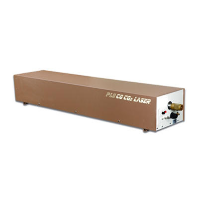
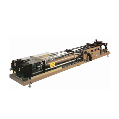
北京欧兰科技发展有限公司为您提供《有机小分子中量子点发射检测方案(激光产品)》,该方案主要用于其他中量子点发射检测,参考标准《暂无》,《有机小分子中量子点发射检测方案(激光产品)》用到的仪器有PL3140 皮秒Nd:YLF激光器。
我要纠错
相关方案
 咨询
咨询