

方案详情文
智能文字提取功能测试中
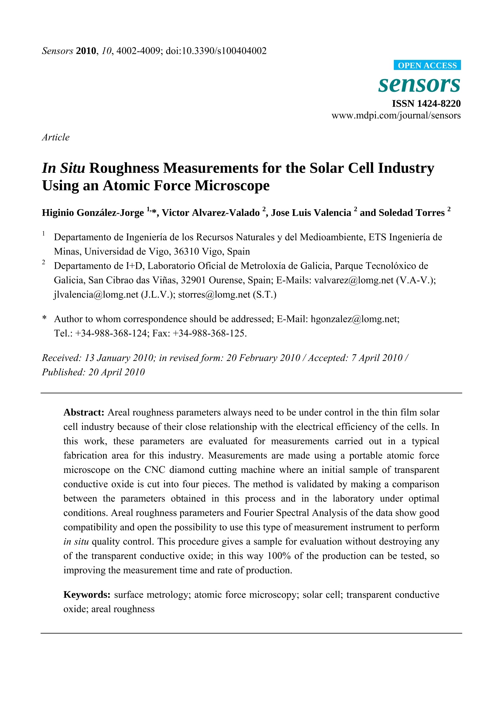
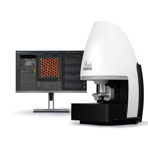
Sensors 2010, 10,4002-4009; doi:10.3390/s100404002OPEN ACCESS 4003Sensors 2010, 10 SensorS ISSN 1424-8220 www.mdpi.com/journal/sensors Article In Situ Roughness Measurements for the Solar Cell IndustryUsing an Atomic Force Microscope Higinio Gonzalez-Jorgel, Victor Alvarez-Valado, Jose Luis Valenciaand Soledad Torres’ Departamento de Ingenieria de los Recursos Naturales y del Medioambiente,ETS Ingenieria deMinas, Universidad de Vigo, 36310 Vigo, Spain 2Departamento de I+D,Laboratorio Oficial de Metroloxia de Galicia, Parque Tecnoloxico deGalicia, San Cibrao das Vinas, 32901 Ourense, Spain; E-Mails: valvarez@lomg.net (V.A-V.);jlvalencia@lomg.net (J.L.V.); storres@lomg.net (S.T.) * Author to whom correspondence should be addressed; E-Mail: hgonzalez@lomg.net;Tel.: +34-988-368-124; Fax: +34-988-368-125. Received: 13 January 2010; in revised form: 20 February 2010 /Accepted: 7 April 2010/Published: 20 April 2010 Abstract: Areal roughness parameters always need to be under control in the thin film solarcell industry because of their close relationship with the electrical efficiency of the cells. Inthis work, these parameters are evaluated for measurements carried out in a typicalfabrication area for this industry. Measurements are made using a portable atomic forcemicroscope on the CNC diamond cutting machine where an initial sample of transparentconductive oxide is cut into four pieces. The method is validated by making a comparisonbetween the parameters obtained in this process and in the laboratory under optimalconditions. Areal roughness parameters and Fourier Spectral Analysis of the data show goodcompatibility and open the possibility to use this type of measurement instrument to performin situ quality control. This procedure gives a sample for evaluation without destroying anyof the transparent conductive oxide; in this way 100% of the production can be tested, soimproving the measurement time and rate of production. Keywords: surface metrology; atomic force microscopy; solar cell; transparent conductiveoxide; areal roughness 1.Introduction Roughness parameters describe the irregularities that occur due to the material removal processes,including tool geometry, wheel grit, electrical discharge machining spark, and chemical or physicalvapor deposition [1-3]. In this sense, roughness parameters are key factors for a number of industrialmanufactured products and directly influence their subsequent performance. Some examples are therelationship of roughness with tribology [4,5], the reflectivity of optical products fabricated bydiamond turning [6] or moulding [7] and the adhesion of paint and plating applications [8]. Areal surface evaluation is of greater interest than 2D profiles. For example, if a random profile istaken from an areal surface measurement, differences between discrete pits and scratches are notrevealed; for this reason the areal image is needed. Restriction in areal surface measurements comesfrom the range and resolution of the instrumentation available, although several kinds of measuringequipment are available for related applications (i.e., atomic force microscopy, optical or stylusprofilometry)[9]. Atomic force microscopes (AFMs) are especially useful when high lateral resolution is required andthe measurement range is small [10]. One of the typical problems relating to this technology is thenecessity to destroy the manufactured part to obtain an evaluation sample, which is moved from thefabrication area to the laboratory area, where the AFM is usually located. Recently some AFMmanufactures have provided instruments that are portable and therefore can, at first sight, be used tomake in situ measurements in industry [11,12]. Moreover, a lot of work must be performed todemonstrate their real behavior in each specific industrial environment. The thin film photovoltaic industry has been growing significantly over recent years, driven by theincreasing demand of photovoltaic power plants and the higher price of silicon. The front panel of thiskind of solar cell consists of a transparent conductive oxide (TCO) material which allows lighttransmission and also serves as an electric contact. TCO roughness is an important parameter inquality control because it is directly related to the electrical efficiency of the module [13,14]. Thisparameter is nowadays usually checked using mechanical profilers (2D roughness) or AFMs (arealroughness). This study is carried out using an evaluation sample which is taken from a TCO panelremoved from the fabrication area. The problems for this method are time consumption, destruction ofthe TCO panel and the impossibility to make a control, at least on a small area, in 100% of production. In this work, we make a metrological comparison between the areal roughness, determined by anAFM measurement on a TCO panel, in both the fabrication and laboratory areas of a solar cellcompany. The aim of this feasibility study is to demonstrate the in situ capability of using thisinstrument for quality control and open the possibility of extending its use. 2.Experimental 2.1.AFMInstrument The AFM used in these experiments is the Nanosurf Easyscan 2 (Figure 1). This AFM head isdifferent to those normally used, which are based on piezoelectric tube scanners, and its motion andmeasurement principles are described below. Figure 1. (A) AFM Nanosurf Easyscan 2 and (B) scene of the scanning tripod. The coarse height of AFM is provided by three large vertical screws (Figure 1-A1) at the edges ofthe unit and this traditional mechanical arrangement is complemented with a motorized movement(Figure 1-A2) that allows the cantilever tip to approach the sample safely. Fine scale x-y-z movementof the cantilever is controlled from inside the head assembly (Figure 1-B). A tripod is suspended onthree flat shaped springs with three iron cylinders (Figure 1-B1) behind them, each spaced a little infront of small electromagnets (Figure 1-B2). Different energy supplied to the electromagnets producesdifferent cantilever motions. For instance, when all the electromagnets are energized together, thecantilever moves straight back. On the other hand, if the right electromagnet is energized the cantilevermoves right. The measurement principle is the same as in traditional AFMs. It consists of the combination of alaser diode (Figure 1-B3), which generates the beam that irradiates the back of the cantilever tip(Figure 1-B4), with the reflected beam analyzed by a photodetector (Figure1-B5). It should be noted that the portable concept has been achieved because the measurement and themotion system are both assembled in the same AFM head. AFM instruments, where the motionactuator is in the horizontal stage and the measurement system is in the head, cannot be used forportable measurements. The horizontal stage (Figure 1-A3) of the AFM can be only used for the measurements made in thecompany laboratory and not when it is acting as a portable instrument in the fabrication area. The measurement parameters selected for these experiments are as follows: Operating mode: Tapping mode Cantilever force: 20 nN Image resolution: 256 points per line (ppl) Lines: 256 Time per line:1 s Cantilever type: Nanosensors NCLR [15] Vibration frequency: 159.4 kHz Measurement time: 8 min 30 s (approximate) 2.2. Validation Process The fabrication area selected for performance of the measurements is on the cutting table becausethis place is relatively isolated from acoustic noise. The cutting table is based on a CNC diamondcutting machine which obtains four TCO panels of 1.35 m’ from the larger one of 5.4 m. Nowadaysareal roughness of the panels is only measured in a small number of them. This quality control processis performed cutting a small part of the panel which is then scanned with the AFM in the laboratory.This panel is then removed from the production line and destroyed. In this paper we try to validate theAFM possibility to perform in situ measurements without destroying the panel, so we establish thefollowing steps: - A region of interest (10 cm) is selected on a large panel (5.4 m’) on the cutting table(Figure2). Five sub-topographies are obtained from this region using the AFM in portable configuration. The region of interest is cut and moved to the laboratory. The laboratory room is isolated fromnoise and vibration and the AFM is placed on an optical table with pneumatic isoltation. Sample in the laboratory is measured and roughness results are compared with those previouslyobtained to demonstrate the possibility or not to use the AFM as portable instrument in thefabrication of a solar cell industry. Figure 2. Measurement configurations in five sub-topographies (A) in situ and (B) inlaboratory. P1-P5 indicate the regions where the sub-topographies were made. ) The areal roughness parameters to be compared for the two measurement configurations areroughness average Sa and roughness root mean square Sq [16]. Data evaluation is performed for all ofthe 65,536 topography points. Mean values and standard deviation are obtained for both fabrication and laboratory measurements, for comparison. In addition, all data were processed using a Fast FourierTransform to make a spectral analysis and compare noise influences between both configurations. 3. Results and Discussion Figure 3 shows the top left sub-topographies (P1 in Figure 2) obtained for the fabrication andlaboratory areas. Figures 4 and 5 depict the evaluation of the areal roughness parameters Sa and Sq,respectively. Table 1 exhibits the values and standard deviation obtained for the areal roughnessaverage and root mean square from the five sub-topographies in the two areas of study. Each profilepoint represents the contribution of 8 lines of the profile (2,048 topography data with 256 ppl). Onlythese values where represented on the plots to avoid overcharging of the computer memory. Figure 3. Top left sub-topographies-P1 obtained (A) in situ and (B) in laboratory. Figure 4. Results for areal roughness parameter Sa (A) in situ and (B) in laboratory. Index 1represents the raw data and 2 the average of the five sub-profiles. Error bars indicate thestandard deviation of the average. Figure 5. Results for areal roughness parameter Sq (A) in situ and (B) in laboratory. Index 1represents the raw data and 2 the average of the five sub-profiles. Error bars indicate thestandard deviation ofthe average. Figures 4 and 5 show a high variability in the roughness parameters during the first profile points,but they tend to converge to one asymptotic value over the fifth profile point (10,240 topography datainvolved in the calculation). This is due to the fact that roughness is a statistical parameter and a highnumber of input data are needed to obtain a good result. Comparison between the roughness parameters (Table 1) reveals good agreement between thefabrication and laboratory areas, demonstrating that in situ measurements can be performed with thisportable AFM. Although the set of samples are the same under the two measurement procedures, it isremarkable that higher standard deviation is obtained from the values in the laboratory area. Asenvironmental conditions are better in laboratory than in factory, the reason for these results are thedifferences of intrinsically roughness values obtained from the sub-topographies. For example inFigure 4-B1 deviation in laboratory come from the roughness value differences betweensub-topographies P1-P5 and not for self topography deviations. Such results are in agreement with theroughness tolerance of the panel (4 nm-manufacturer data), so this source of error can only arisefrom the sample non-uniformity and not from instabilities in the measurement procedure or tipartifacts. Previous experiments made for our group show as changes in roughness measurements usingdifferent tips are under the tolerance of the own TCO material. To complete the study a Fourier Spectral Analysis [1] was made for all the sub-topographies(Figure 6). Both situations show a similar pattern, which demonstrates a similar influence from smallwavelength noise (typically from sound pressure level or vibrations) or long wavelength noise(typically from temperature fluctuations). Table 1. Areal values and standard deviation of roughness average and roughness rootmean square obtained from the five sub-topographies in the fabrication and laboratory areas. Fabrication area Laboratory area Sa (nm) 27.4±0.6 26.6±1.7 Sq (nm) 34.9±0.6 34.1±2.4 Figure 6. Fourier Spectral Analysis for measurements performed (A) in situ and (B)in laboratory. In process measurement Laboratory measurement 4. Conclusions This research work shows a comparative study between several parameters obtained using an AFMacting as a portable instrument in the fabrication area of the solar cell company and placed in thelaboratory area, where tip influence is not relevant for the rough TCO samples. Results obtained inboth situations are in agreement and they show the capability of using this instrument for in situmeasurements. This new configuration would reduce the time required for quality control, because thesample does not have to be moved to the laboratory and avoids the need to destroy the TCO panel toobtain an evaluation sample, 100% of the production output may be inspected. This study tries to be afirst approach to open the possibility to use this kind of instrumentation under fabrication conditions.Much work must be make for the future as for example to study the behavior of different AFMinstruments or study how the hard working conditions affect to AFM metrological stability. Acknowledgements Authors would like to give thanks“Xunta de Galicia" for the financial support (project code08DPI016CT and human resources program Lucas Labrada and Angeles Alvarino).They also givethanks to Leonardo de Chiffre from Technical University of Denmark, Jacinto Perez from TSOLAR. References and Notes 1. Smith, G.T. Industrial Metrology: Surfaces and Roundness; Springer-Verlag:London, UK, 2002. 2. Dagnall, M.A. Exploring Surface Texture; Rank Taylor Hobson Limited: Leicester, UK, 1986. 3. Whitehouse, D.J. Handbook of Surface and Nanometrology; Institute of Physics Publishing:London,UK,2003. 4. Eckardt,T.; Bewilogua, K.; van der Kolk, G.; Hurkmans, T.; Trinh, T.; Fleisher, W. Improvingtribological properties of sputtered boron carbide coatings by process modifications. Surf. Coat.Tech. 2000, 126,69-75. 5. Begand, S.; Oberbach, T.; Herrmann, M.; Sempf, K. Surface properties after ageing of dispersionceramic and its influence on strength. Key Eng. Mat.2009,396-398,157-160. 6. Gubbels, G.; van Venrooy, B.; Bosch, A.J.; Senden, R. Rapidly solidified aluminium for opticalapplications. In Proceedings of the SPIE-The international society for optical engineering,Marseille, France,2008; pp. 70183-70192. 7. Masuda, J.; Yan, J.; Tashiro, T.; Fukase, Y.; Zhou, T.; Kuriyagawa, T. Microstructural andtopographical changes of Ni-P plated moulds in glass lens pressing. Int. J. Surf. Sci. Eng. 2009,3,86-102. 8. Sakata, F.Y.; Santo, A.M.E.; Miyakawa, W.; Riva, R.; Lima, M.S.F. Influence of laser surfacetexturing on surface microstructure and mechanical properties of adhesive joined steel sheets. Surf.Eng. 2009,25,180-186. 9. Brown, L.; Blunt, L. Surface metrology for the automotive industry. In Proceedings ofInauguralAutomotive Researchers Conference, Huddersfield, UK, 2008. 10.DIanzebrink, H.U.; Koenders, L.; Wikening, G.; Yacoot, A.; Kunzmann, H. Advances in scanningforce microscopy for dimensional metrology. CIRP Ann.-Manuf. Technol. 2006, 55,841-878. 11. Nanosurf, Available online: http://www.nanosurf.com/default.cfm?curr navi=11&curr_content=11&spr=en(Access on 22 Decemeber 2009). 12.IDME Scanning Probe Microscopes, Available online: http://www.dme-spm.com/ds95.html(Access on 26 December 2009). 13. Krc,J.; Zeman, M.; Kluth,O.; Smole, F.; Topic, M. Effect of surface roughness of ZnO: Al filmson light scattering in hydrogenated amorphous silicon solar cells. Thin solid films 2003, 426, 296-304. 14.Escarre, J.; Villar, F.; Fonrodona, M.; Soler, D.; Asensi, J.M.; Bertomeu, J.; Andreu, J. Opticalanalysis of textured plastic substrates to be used in thin silicon solar cells. Solar Energ. Mater.Solar Cells,2005,87,333-341. 15. Nanosensors, Available online: http://www.nanosensors.com/PPP-NCLR.htm (Access on 1lDecember 2009). 16. Image Metrology, http://www.imagemet.com/WebHelp/spip.htm#roughness_parameters.htm(Access on 22 December 2009). C 2010 by the authors; licensee MDPI, Basel, Switzerland. This article is an open-access articledistributed under theterms and conditionsof the Creative Commons Attribution1license(http://creativecommons.org/licenses/by/3.0/). Nanite 原子力显微镜系统是纳米测量和成像的完美工具。该系统提供三维数据。原子力显微镜测量是非破坏性的,无需制备样品。此外,机械运动平台允许批量的,预编程测量,使用大型花岗岩自动X/Y/Z样品台可测试尺寸达180mm样品的不同区域,用户甚至可以定制更大的移动样品台。Nanite设计灵活、操作简单,是您理想的全自动研究级AFM系统。瑞士Nanosurf公司,全球知名的专业研发扫描探针原子力显微镜制造商和技术服务供应商,在扫描探针原子力显微镜领域有超过15年的研发经验,一直致力于新型扫描探针原子力显微镜的创新性研发和制造。目前已推出新一代低噪音-快速扫描-超高稳定性的AFM 和大扫描范围Nanite AFM系统。瑞士Nanosurf公司承诺提供最高品质的服务和客户支持,同时还提供纳米技术的OEM 客户定制,外包等业务。技术参数:原子力显微镜测量模式: 接触式原子力显微镜,真正非接触式原子力显微镜,横向力/摩擦力显微镜(LFM),导电原子力显微镜,磁力显微镜(MFM),开尔文探针(Kelvin Probe),扫描热原子力显微镜(SThM),电容和静电力显微镜(EFM),高级的纳米光刻和纳米操作能力,音叉原子力显微镜,三维扫描成像。 ● 原子力显微镜扫描器最大测量范围:110um X & Y range,22um Z range ● 大尺寸样品台,全自动测量最大直径为160mm样品。 ● PZT/Voice Coil双模式技术AFM ● 全自动运动平台,马达驱动 ● 专利批处理软件,自动图像拼接缝合技术,可以测量超大样品的三维形貌像 ● 先进的32-bit DSP控制器,专利反馈技术(扫描范围>10um时最高扫描20 Hz,消除爬行现象) ● 可以进行纳米压痕和划痕实验 ● 专利光学系统, XY闭环扫描技术 ● 独特开放性软硬件构架设计, 并开放所有源代码供您的二次开发主要特点:● 原子力显微镜扫描器最大测量范围:110um X & Y range,22um Z range● 大尺寸样品台,全自动测量最大直径为160mm样品。● PZT/Voice Coil双模式技术AFM● 全自动运动平台,马达驱动● 专利批处理软件,自动图像拼接缝合技术,可以测量超大样品的三维形貌像● 先进的32-bit DSP控制器,专利反馈技术(扫描范围>10um时最高扫描20 Hz,消除爬行现象)● 可以进行纳米压痕和划痕实验● 专利光学系统, XY闭环扫描技术● 独特开放性软硬件构架设计, 并开放所有源代码供您的二次开发
关闭-
1/8
-
2/8

还剩6页未读,是否继续阅读?
继续免费阅读全文
北京亿诚恒达科技有限公司为您提供《薄膜太阳能中测量和评价粗糙度参数检测方案(扫描探针)》,该方案主要用于太阳能中测量和评价粗糙度参数检测,参考标准《暂无》,《薄膜太阳能中测量和评价粗糙度参数检测方案(扫描探针)》用到的仪器有原子力显微镜。
我要纠错
推荐专场
扫描探针显微镜SPM(原子力显微镜AFM、扫描隧道显微镜STM)
更多
相关方案
 咨询
咨询