

方案详情文
智能文字提取功能测试中
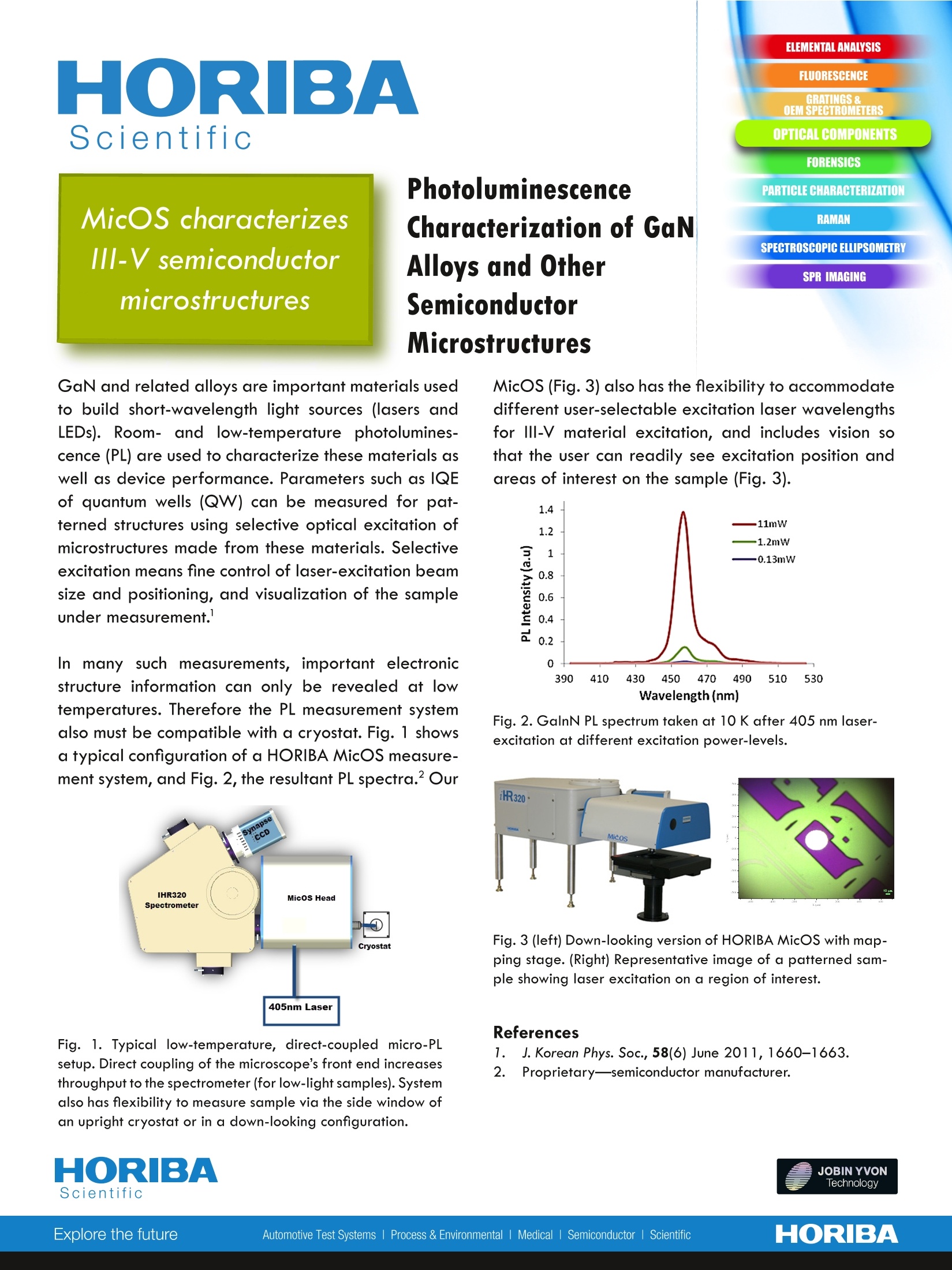
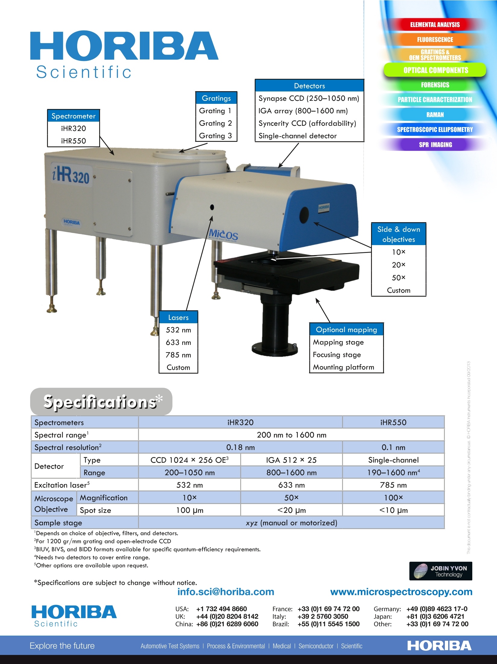
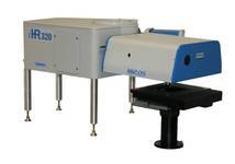
MicOS characterizesIII-V semiconductormicrostructures PhotoluminescenceCharacterization of GaNAlloys and OtherSemiconductorMicrostructures GaN and related alloys are important materials usedto build short-wavelength light sources (lasers andLEDs). Room- and low-temperature photolumines-cence (PL) are used to characterize these materials aswell as device performance. Parameters such as IQEof quantum wells (QW) can be measured for pat-terned structures using selective optical excitation ofmicrostructures made from these materials. Selectiveexcitation means fine control of laser-excitation beamsize and positioning, and visualization of the sampleunder measurement. Inmany such measurements, important electronicstructure information can only be revealed at lowtemperatures. Therefore the PL measurement systemalso must be compatible with a cryostat. Fig. 1 showsa typical configuration of a HORIBA MicOS measure-ment system, and Fig. 2, the resultant PL spectra.Our Fig. 1. Typical low-temperature, direct-coupled micro-PLsetup. Direct coupling of the microscope’s front end increasesthroughput to the spectrometer (for low-light samples). Systemalso has flexibility to measure sample via the side window ofan upright cryostat or in a down-looking configuration. MicOS (Fig. 3) also has the flexibility to accommodatedifferent user-selectable excitation laser wavelengthsfor ⅢI-V material excitation, and includes vision sothat the user can readily see excitation position andareas of interest on the sample (Fig.3). Fig. 2. GalnN PL spectrum taken at 10 K after 405 nm laser-excitation at different excitation power-levels. Fig. 3 (left) Down-looking version of HORIBA MicOS with map-ping stage. (Right) Representative image of a patterned sam-ple showing laser excitation on a region of interest. References J. Korean Phys. Soc.,58(6) June 2011,1660-1663.2 Proprietary—semiconductor manufacturer. Specifications* Spectrometers iHR320 iHR550 Spectral range 200 nm to 1600 nm Spectral resolution² 0.18nm 0.1 nm Detector iype CCD 1024×256 OE IGA 512×25 Single-channel Range 200-1050 nm 800-1600 nm 190-1600 nm4 Excitation laser 532 nm 633 nm 785nm Microscope Objective Magnification 10× 50× 100× Spot size 100 pm <20 pm <10 um Sample stage xyz (manual or motorized) O工moc Depends on choice of objective, filters, and detectors. For 1200 gr/mm grating and open-electrode CCD E50 3BIUV, BIVS, and BIDD formats available for specific quantum-efficiency requirements. 4Needs two detectors to cover entire range. Other options are available upon request. *Specifications are subject to change without notice. info.sci@horiba.com www.microspectroscopy.com UK: +44 (0)20 8204 8142 Italy: +39 2 5760 3050 Japan: +81 (0)3 62064721 PIO China: +86 (0)21 6289 6060 Brazil: +55 (0)11 5545 1500 Other: +33(0)16974 7200 JOBIN YVONTechnologyHORIBAExplore the futureAutomotive Test Systems Process & EnvironmentalMedical SemiconductorrlScientific
关闭-
1/2
-
2/2
产品配置单
HORIBA(中国)为您提供《MicOS应用于III-V族半导体材料光致发光及微结构检测 》,该方案主要用于其他中null检测,参考标准《暂无》,《MicOS应用于III-V族半导体材料光致发光及微结构检测 》用到的仪器有MicOS显微光谱测量系统。
我要纠错
推荐专场
其它光谱仪
更多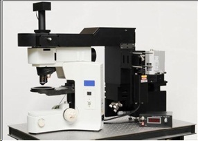
相关方案
 咨询
咨询