

方案详情文
智能文字提取功能测试中
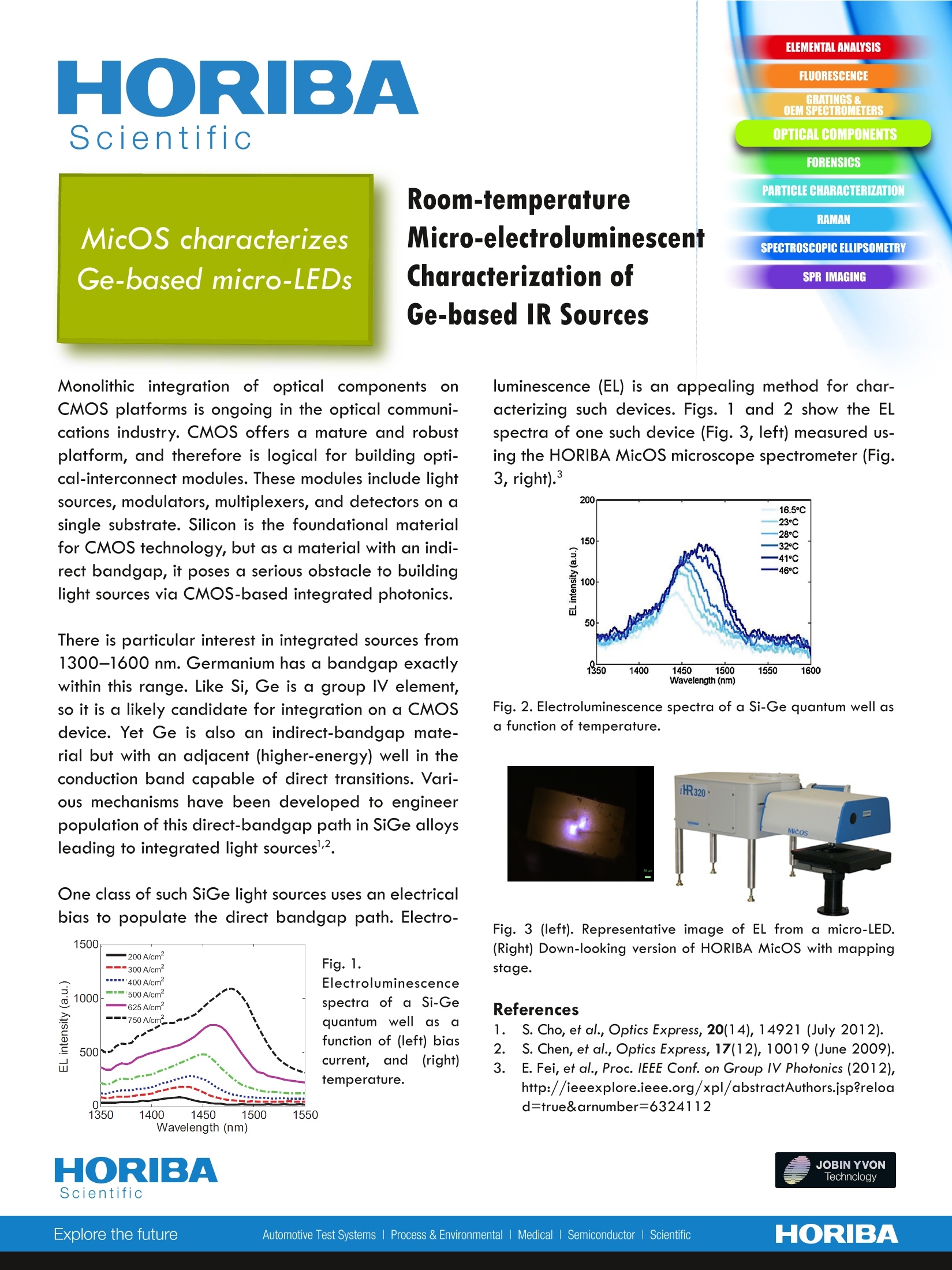
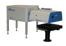
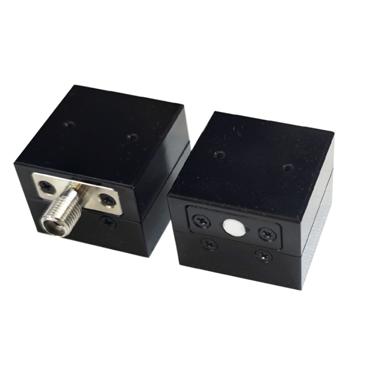
MicOS characterizesGe-based micro-LEDs Room-temperatureMicro-electroluminescentCharacterization ofGe-based IR Sources Monolithic integration of optical componentsonCMOS platforms is ongoing in the optical communi-cations industry. CMOS offers a mature and robustplatform, and therefore is logical for building opti-cal-interconnect modules. These modules include lightsources, modulators, multiplexers, and detectors on asingle substrate. Silicon is the foundational materialfor CMOS technology, but as a material with an indi-rect bandgap, it poses a serious obstacle to buildinglight sources via CMOS-based integrated photonics. There is particular interest in integrated sources from1300-1600 nm. Germanium has a bandgap exactlywithin this range. Like Si, Ge is a group lV element,so it is a likely candidate for integration on a CMOSdevice. Yet Ge is also an indirect-bandgap mate-rial but with an adjacent (higher-energy) well in theconduction band capable of direct transitions. Vari-ous mechanisms have been developed to engineerpopulation of this direct-bandgap path in SiGe alloysleading to integrated light sources'. One class of such SiGe light sources uses an electricalbias to populate the direct bandgap path. Electro- Fig. 1. Electroluminescencespectra of a Si-Gequantum well as afunction of (left) biascurrent, and (right)temperature. 1550 luminescence (EL) is an appealing method for char-acterizing such devices. Figs. 1 and 2 show the ELspectra of one such device (Fig. 3, left) measured us-ing the HORIBA MicOS microscope spectrometer (Fig.3,right). Fig. 2. Electroluminescence spectra of a Si-Ge quantum well asa function of temperature. Fig. 3(left). Representative image of EL from a micro-LED.(Right) Down-looking version of HORIBA MicOS with mappingstage. References .S. Cho, et al.,Optics Express, 20(14), 14921 (July 2012).23 .S.S. Chen, et al., Optics Express, 17(12), 10019 (June 2009). E. Fei, et al., Proc. IEEE Conf. on Group IV Photonics (2012),http://ieeexplore.ieee.org/xpl/abstractAuthors.jsp?reload=true&arnumber=6324112 Specifications* Spectrometers iHR320 iHR550 Spectral range 200 nm to 1600 nm Spectral resolution² 0.18nm 0.1 nm Detector iype CCD 1024×256 OE IGA 512×25 Single-channel Range 200-1050 nm 800-1600 nm 190-1600 nm4 Excitation laser 532nm 633 nm 785 nm Microscope Objective Magnification 10× 50× 100× Spot size 100 pm <20 pm <10 um Sample stage xyz (manual or motorized) O工moc 'Depends on choice of objective, filters, and detectors. For 1200 gr/mm grating and open-electrode CCD E50 3BIUV, BIVS, and BIDD formats available for specific quantum-efficiency requirements. 4Needs two detectors to cover entire range. Other options are available upon request. *Specifications are subject to change without notice. info.sci@horiba.com www.microspectroscopy.com UK: +44 (0)20 8204 8142 Italy: +39 2 57603050 Japan: +81 (0)3 62064721 PO China: +86 (0)21 6289 6060 Brazil: +55 (0)11 55451500 Other: +33 (0)1 69 74 72 00 JOBIN YVONTechnologyHORIBAExplore the futureAutomotive Test Systems Process & EnvironmentalMedical SemiconductorrlScientific
关闭-
1/2
-
2/2

产品配置单
HORIBA(中国)为您提供《MicOS应用于微型LED电致发光检测》,该方案主要用于其他中null检测,参考标准《暂无》,《MicOS应用于微型LED电致发光检测》用到的仪器有MicOS显微光谱测量系统。
我要纠错
推荐专场
其它光谱仪
更多
相关方案
 咨询
咨询