

方案详情文
智能文字提取功能测试中
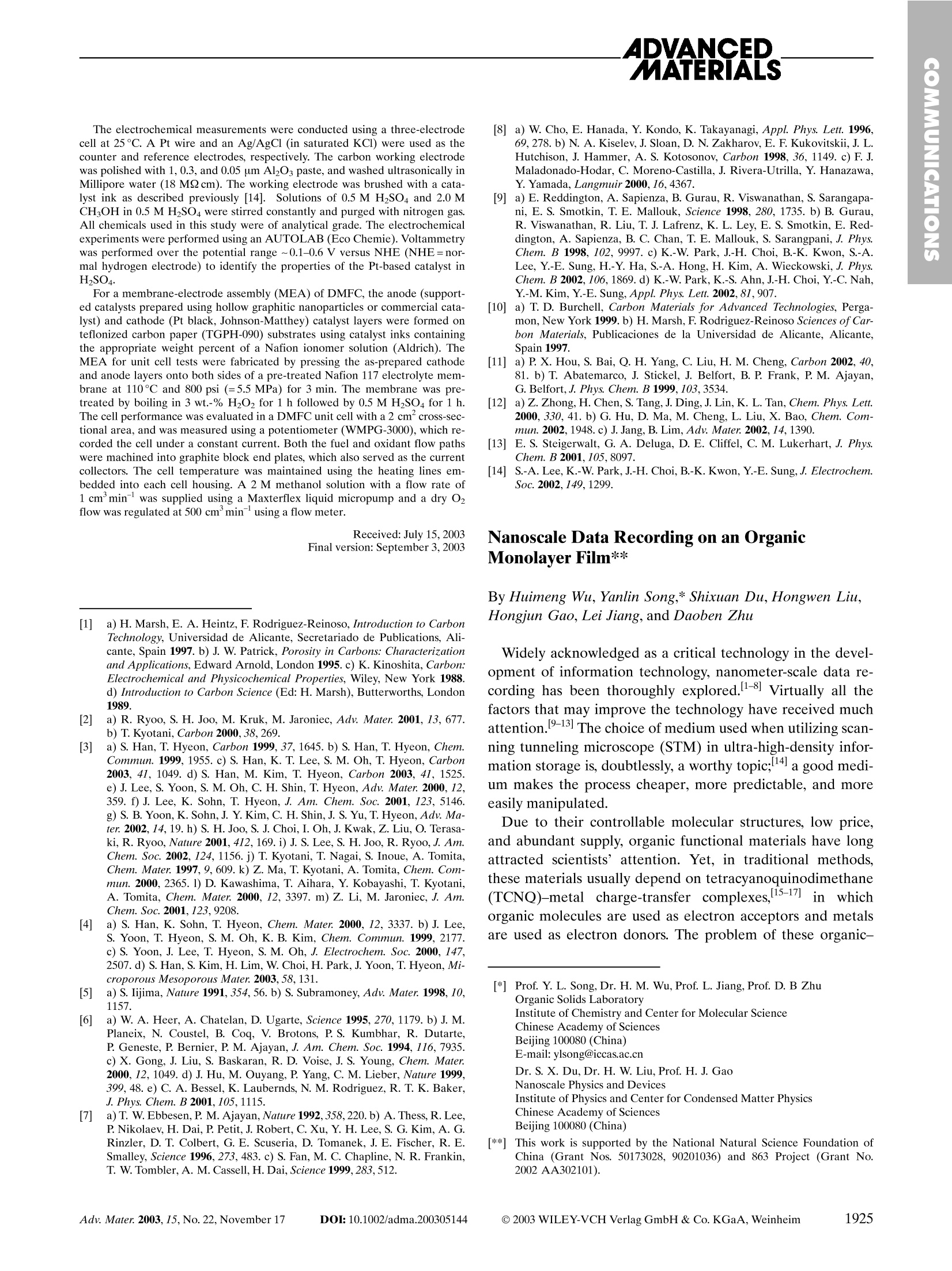
ADVANCED,MATERALS The electrochemical measurements were conducted using a three-electrodecell at 25C. A Pt wire and an Ag/AgCl (in saturated KCl) were used as thecounter and reference electrodes, respectively. The carbon working electrodewas polished with 1, 0.3, and 0.05 um Al2O3 paste, and washed ultrasonically inMillipore water (18 MQ cm). The working electrode was brushed with a cata-lyst ink as described previously [14]. Solutions of 0.5 M H2SO4 and 2.0 MCH,OH in 0.5 M HSO4 were stirred constantly and purged with nitrogen gas.All chemicals used in this study were of analytical grade. The electrochemicalexperiments were performed using an AUTOLAB (Eco Chemie). Voltammetrywas performed over the potential range ~0.1-0.6 V versus NHE (NHE=nor-mal hydrogen electrode) to identify the properties of the Pt-based catalyst inH SO4. For a membrane-electrode assembly (MEA) of DMFC, the anode (support-ed catalysts prepared using hollow graphitic nanoparticles or commercial cata-lyst) and cathode (Pt black, Johnson-Matthey) catalyst layers were formed onteflonized carbon paper (TGPH-090) substrates using catalyst inks containingthe appropriate weight percent of a Nafion ionomer solution (Aldrich). TheMEA for unit cell tests were fabricated by pressing the as-prepared cathodeand anode layers onto both sides of a pre-treated Nafion 117 electrolyte mem-brane at 110°C and 800 psi (=5.5 MPa) for 3 min. The membrane was pre-treated by boiling in 3 wt.-% H2O2 for 1 h followed by 0.5 M HSO4 for 1 h.The cell performance was evaluated in a DMFC unit cell with a 2 cmcross-sec-tional area, and was measured using a potentiometer(WMPG-3000), which re-corded the cell under a constant current. Both the fuel and oxidant flow pathswere machined into graphite block end plates, which also served as the currentcollectors. The cell temperature was maintained using the heating lines em-bedded into each cell housing. A 2 M methanol solution with a flow rate of1 cm’min- was supplied using a Maxterflex liquid micropump and a dry O2flow was regulated at 500 cm’min-using a flow meter. ( R eceived: July 15, 2003 F inal version: September 3, 2003 ) [1] a) H. Marsh, E. A. Heintz, F. Rodriguez-Reinoso, Introduction to CarbonTechnology, Universidad de Alicante, Secretariado de Publications, Ali-cante, Spain 1997. b) J. W. Patrick, Porosity in Carbons: Characterizationand Applications, Edward Arnold, London 1995.c) K. Kinoshita, Carbon:Electrochemical and Physicochemical Properties, Wiley, New York 1988.d) Introduction to Carbon Science (Ed: H. Marsh), Butterworths, London1989 [2] a) R. Ryoo, S. H. Joo, M. Kruk, M. Jaroniec, Adv. Mater. 2001,13,677.b) T. Kyotani, Carbon 2000, 38,269. ( [3] a ) S . Han, T. Hyeon, Ca r bon 1999, 3 7 , 1 6 45. b) S. Han, T. H yeon, Chem.Commun. 1999, 1955.c) S. Han, K. T. Lee, S. M. O h, T. Hyeon, Carbon2003, 41, 1049. d) S . Han, M. Kim, T. Hyeon, C arbon 2 0 03, 41,1 5 25.e) J . Lee, S. Yoon, S . M . Oh, C. H. Shin, T. Hyeon, Adv. Mat e r. 2000 , 12, 359. f ) J. Lee, K. Sohn, T. Hyeon, J. Am. Chem. S o c. 2 0 01, 1 2 3, 5 1 46. g ) S . B. Yoon, K. Sohn, J. Y . K im, C. H . Shin, J. S. Yu,T . Hyeon, Adv. Ma- t er. 2002, 1 4,1 9 .h) S. H . Joo, S. J. C hoi, I. Oh, J. Kwak, Z . L i u, O. Terasa- k i, R. Ryoo,N a ture 2001,412,169.i) J . S. Lee, S. H. Joo, R. Ryoo,J. Am.Chem. Soc.2002,12 4 ,1156. j) T . Kyotani, T. N a g a i, S. I noue, A. Tomita,Chem. Mater. 1997,9,609.k) Z. Ma, T. K y otani, A. Tomita, C h em. Com-mun.2 0 00, 2365.1) D. Ka w ashima, T. A i h a ra, Y. K o bayashi, T. K y otani,.A. Tomita, Chem. M ater. 2 000, 1 2, 3397. m) Z. L i, M. J aroniec, J. Am.Chem. Soc. 2001,123,9208. ) ( 4 a ) S . Han, K . Sohn, T. Hyeon, Che m . Ma t er. 2000, 12, 33 3 7. b) J. L e e,S. Yoon, T. Hyeon, S. M . Oh, K. B. Kim, Chem. Commun. 1999, 2 177. c ) S. Yoon, J. L ee, T. H yeon, S. M . Oh , J. El e ctrochem. Soc. 2000, 147, 2 507.d)S. Han, S . Kim, H. L i m, W. Choi, H . Park, J. Yoon, T . Hyeon, Mi-croporous Mesoporous Mater. 2 0 03,58,13 1 . .PO C ) ( [5] a) S. Iijima, Nature 1991,354,56. b) S. Subramoney, Adv. Ma t er.199 8 ,10,1157. ) ( [6] a ) W . A. Heer, A . Chatelan, D. Ug a rte, Science 1995, 270,1179. b) J. M. Planeix, N. Coustel, B. Coq, V. B rotons, P. S . K umbhar, R . Du t arte, P . Geneste, P. Bernier, P. M. Ajayan, J. Am. Chem. S oc. 1 994,1 1 6,7935.c) X. G ong, J . Liu, S . B askaran, R . D . V o ise, J. S. Y oung, C h em. Mater.2000, 1 2,1 0 49. d)J. Hu, M . Ouyang, P. Y a n g, C. M. L ieber, Nature 1999 , 399,48. e) C . A. Bessel, K. Laubernds, N. M. Ro d riguez, R. T . K . B ak e r,J. Phys . Chem. B 2001 , 105,1115. ) ( [7] a) T . W . E bbesen, P. M . Ajayan, Nature 1992,358,220. b) A. Thess, R. Lee, P .Nikolaev, H. Dai, P . Petit, J. Robert, C. Xu, Y. H. Lee, S. G. Kim, A. G. R inzler, D . T . C olbert , G . E. S cuseri a , D . T omanek, J. E . F i scher, R . E . Smalley, Science 1 9 96, 273, 4 8 3. c ) S. Fan, M. C . Chapline, N. R. Frankin, T. W. Tombler, A. M. Cassell,H . D a i, Science 1999,283, 512. ) ( [8] a ) W . Cho, E . H a nada, Y. Kondo, K. Taka y anagi, Appl. Phys. Lett. 1996 , 69,278. b) N. A. K i selev, J. S loan, D . N. Zakharov, E. F. Kukovitskii, J. L . Hutchison, J. Hammer, A . S. K o tosonov, Carbon 19 9 8, 36 , 114 9 . c) F.J.Maladonado-Hodar, C. Moreno-Castilla, J. Ri v era-Utrilla, Y. H a nazawa,Y. Yamada, Langmuir 2000,16,4367. ) ( [9] a) E. R eddington, A . S a pienza, B . G u rau, R. Viswanathan, S. Sarangapa- n i, E. S. Smotkin, T. E. Mallouk, S cience 1 998, 280, 1 735. b ) B. G urau, R . V iswanathan, R . Li u , T. J. L a frenz, K . L. L e y, E. S . S m otkin, E. Re d - dington, A. S apienza, B . C. Chan, T. E. M allouk, S. Sarangpani, J. P hys. Chem. B 1 9 98,102, 9997. c ) K.-W. P a rk, J.-H. C hoi, B .-K. K won, S.-A.Lee, Y .-E. S ung, H .-Y. Ha, S.-A. Hong, H. Kim, A. Wieckowski, J. Phys.Chem. B 2002, 106,18 6 9.d) K.- W . Park, K.-S. Ahn , J.-H. Cho i , Y.-C. Nah, Y .-M. Kim, Y.-E. Sung, Appl. P h ys. Lett. 2002,81,90 7 . ) [10]a) T. D. Burchell, Carbon Materials for Advanced Technologies, Perga-mon, New York 1999. b) H. Marsh, F. Rodriguez-Reinoso Sciences of Car-bon Materials, Publicaciones de la Universidad de Alicante, Alicante,Spain 1997. [11]a) P. X. Hou, S. Bai, Q. H. Yang, C. Liu, H. M. Cheng, Carbon 2002, 40,81. b) T. Abatemarco, J. Stickel, J. Belfort, B. P. Frank, P.M. Ajayan,G. Belfort,J. Phys. Chem. B 1999,103,3534. ( [12] a) Z. Zhong, H. Chen, S. Tang, J. Ding, J. Lin, K. L . Tan, Chem. Phys. Lett.2000,330,41. b) G. Hu, D. Ma, M. Cheng, L. Liu, X. Bao, Chem. Com-mun. 2002,1948.c) J . Jang, B. Lim, Adv. Mater.2002,14,1390. ) [13]l EE. S. Steigerwalt, G. A. Deluga, D. E. Cliffel, C. M. Lukerhart, J. Phys.Chem. B 2001,105,8097. [14]S.-A. Lee, K.-W. Park, J.-H. Choi, B.-K. Kwon, Y.-E. Sung, J. Electrochem.Soc. 2002,149,1299. Nanoscale Data Recording on an OrganicMonolayer Film** By Huimeng Wu, Yanlin Song,* Shixuan Du, Hongwen Liu,Hongjun Gao, Lei Jiang, and Daoben Zhu Widely acknowledged as a critical technology in the devel-opment of information technology, nanometer-scale data re-cording has been thoYirroughly explored.[1-8] Virtually all thefactors that may improve the technology have received muchattention.19-13] The choice of medium used when utilizing scan-ning tunneling microscope (STM) in ultra-high-density infor-mation storage is, doubtlessly, a worthy topic; 14] a good medi-um makes the process cheaper, more predictable, and moreeasily manipulated. Due to their controllable molecular structures, low price,and abundant supply, organic functional materials have longattracted scientists’ attention. Yet, in traditional methods,these materials usually depend on tetracyanoquinodimethane(TCNQ)-metal charge-transfer complexes, 15-17inwhichorganic molecules are used as electron acceptors and metalsare used as electron donors. The problem of these organic- ( [ *] P rof. Y . L . S ong,D r . H. M. Wu, Pro f . L. Jiang, Prof. D. B Z hu Organic Solids L a boratory I nstitute o f Chemistry and Center for Molecular Science Chinese Academy of SciencesBeijing 100080 (China)E-mail: ylsong@iccas.ac.cn Dr. S. X. Du, Dr. H. W. Liu,Prof.H . J . Gao Nanoscale P hysics and Devices I nstitute of Physic s and Center for Condensed Matter Physics Chinese Academy of SciencesBeijing 100080 (China) ) ( [** ] T h T is work is s upported b y t he N ational Natural Science Foundation of China (Grant Nos. 50173028, 9 0201036) a nd 8 63 P roject (Grant No.2002 AA302101). ) metal complexes is their inhomogeneous local properties andthe difficulty in making well-dispersed films from them. In contrast to organic-metal complexes, however, all-organ-ic films possess uniform physical-chemical properties. So far,we have successfully designed and synthesized a series of or-ganic complexes, which are stable at ambient temperaturesand pressures. Made into organic thin films, we have testedand confirmed the validation of their use in STM nanometer-scale data storage. 18-22 Of all the results we have observed inour experiments with this series, the smallest mark size was0.6 nm, produced on the organic film of p-nitrobenzonitrile(PNBN).[23] In the PNBN system,-NO2 and -CN are bothstrong electron acceptors, and the recording mechanism maybe ascribed to the molecular structure change in the thin film.Yet, because of the strong repellent interaction betweenPNBN molecules, it is hard to form high-quality films fromsuch molecules. On the other hand, the molecules with elec-tron donors and acceptors usually readily form orderly filmsdue to intermolecular attraction. Therefore, we synthesizedN'-(3-nitrobenzylidene)-p-phenylene-diamine (NBPDA),amolecule with an electron acceptor,-NO2,and an electrondonor, -NH2. We also demonstrated ultra-high-density datastorage in the NBPDA system. 24 Like PNBN, NBPDA is notsuitable for use data recording:it is not stable enough to serveas a recording medium. In order to avoid the defects of the above materials, wehave designed and synthesized the other new organic materialN,N’'-dimethyl-N'(3-nitrobenzylidene)-p-phenylene-diamine(DMNBPDA, see the molecular formula below), which is amolecule with a strong electron donor, -N(CH3)2, and anelectron accepter,-NO2, and more stable than NBPDA (thedonor -NH2 of NBPDA, which is sensitive to air,is protectedby two -CH groups, and the melting point of DMNBPDA israised to 172℃, 26℃ higher than that of NBPDA). Itsorderly thin films for nanometer-scale data recording wereprepared, and the corresponding recording mechanism is alsodiscussed. DMNBPDA was synthesized by our group, and its singlecrystal was prepared and characterized.25] Its thin films weredeposited on freshly cleaved highly ordered pyrolytic graphite(HOPG) substrates by a vacuum-deposition method. In theSTM measurements, the films showed good bistability. Byapplying proper pulsed voltages between the STM tip and thesubstrate, we succeeded in writing a letter “y" on theDMNBPDA film (Fig.1a). The average diameter of themarks is 1.1 nm, and the distance between two dots can reach1.5 nm. The corresponding data-storage density is more than1013bits cm. In order to understand the recording mechanism, local I-Vcharacteristics of the DMNBPDA thin film were measuredbefore and after the voltage pulsing. Figure 1b shows the (a) (b) Fig. 1. a) A“y”formed by nine dots on the DMNBPDA thin film. STM workedin constant height mode. The scanning condition is Vbias=0.36 V, Iref=0.21 nA.The average size of marks in diameter is 1.1 nm; b) the typical current-voltagecurves of the unrecorded and recorded regions in the DMNBPDA thin film.Curve I is related to the recorded region and curve II is related to the unrec-orded region typical local I-V characteristics of the film. It can be seen thatthe electrical resistance of the unrecorded region is muchhigher than that of the recorded region, which means that aconductance transition occurs after the voltage pulse is madeon the film. The I-V experimental result is consistent withour previous speculation that the recording mechanismwas due to charge transfer in the recorded regions.[24,26]The coexistence of strong electron accepter,-NO2, and donor,-N(CH3)2,in the molecule suggests that electron delocaliza-tion may be induced by charge transfer in the recorded regionin the thin film. Generally, charge transfer includes both intra-molecular and intermolecular transfer. In our case, however,the former approach could hardly be responsible becauseintramolecular charge transfer is unstable while the recordingmarks are observed to be extremely stable, with no apparentchange during 10 h scanning. We therefore feel justified inattributing the recording mechanism to intermolecular chargetransfer. To confirm the mechanism, the UV-vis spectra of theDMNBPDA thin film was compared with that of the filmafter the action of an electric field using a standard four-probemethod with a threshold voltage of 8.2 V, see Figure 2. Thespectra of Figures 2a,b exhibit a band with Amax at 397 nmand 399 nm, corresponding to the absorption of DMNBPDAmolecules without interaction among molecules, while thespectrum after the electrical field exhibits two additionalbands at 495 nm and 629 nm besides the peak at 399 nm(Fig. 2b). The new bands are attributed to the intensive inter- Wavlength (nm) Fig. 2. The UV-vis spectra of the DMNBPDA thin film a) before and b) afterapplication of an electrical field. action among molecules, especially intermolecular chargetransfer.[27,28] Considering the Sspecial structure ofDMNBPDA, i.e., the strong electron acceptor and electrondonor in the molecule, the interaction is reasonably due to theintermolecular charge transfer. The charge density distributions of DMNBPDA were calcu-lated using hybrid Hartree-Fock//density-functional-theory(HF//DFT) molecular method of B3LYPI29.30] with 6-31G*basis set.31] The result is shown in Figure 3a, which indicatesthat electron transfer may take place in two nearest-neighbor-ing molecular systems from-N(CH3)2 to-NO2, when inducedby an electric field.The result also shows the highest occupiedmolecular orbital (HOMO) and lowest unoccupied molecularorbital (LUMO) are symmetric, as shown in Figures 3b,c. Thisresult demonstrates the possibility that the HOMO of onemolecule may interact with the LUMO of its neighboringmolecule for charge transfer. Thus, the recording mechanismcan be explained as follows: when a crucial voltage pulse isapplied to the film, charge is transferred from -N(CH3)2 ofone molecule to -NO2 of another molecule,i.e., thej electronis delocalized in the system, and the resistance of the systemis relatively decreased. (a) (b) Fig. 3. a) Charge density distributions of DMNBPDA (the solid circle is positivecharge, and the hollow circle is representative of negative charge); b) HOMOand c) LUMO of DMNBPDA. The analysis of the thin film may be helpful to further un-derstand the recording mechanism. In the observation ofatomic force microscopy (AFM) in Figures 4a,b, we find thatthe top surfaces of the films are very smooth and have somesteps on the films. From the analysis of the topography andphase image, it is clear that the topographically higher places(bright place in phase image) is DMNBPDA thin film and therelatively low places in topography (dark places in phase im-age) are HOPG. The line profile analysis reveals the stepheight to be about 1.4 nm (Figs. 4a,b), almost coincident withthe full molecular length of DMNBPDA (1.36 nm, shown inFigure 4c). This suggests that the organic film is a monolayerand that the DMNPBDA molecules may stand perpendicularto the surface of the HOPG. Figure 4d is a typical molecular-resolution STM image. Using the same tip, an atomic imageof an HOPG sample can be observed easily. From Figure 4d,we find that the molecules of DMNBPDA are arranged peri-odically and the dimension of the periodic unit is 0.43 nmx0.54 nm. Considering the intermolecular charge transfer, wethink the molecules are arranged inversely. Figure 4e showsthe model for arrangement of the molecules on the film. Theorderly arrangements of the organic molecules may arise fromvarious factors such as the nature of the organic molecules,the electrostatic interaction between the neighboring mole-cules, and the function of the substrate. In fact, the orderlyarrangement of DMNBPDA thin film is very important for (b) (c) (d) (e) data storage. In a few experiments, it was troublesome towrite data on the thin films under the same conditions, and itwas also difficult to obtain a molecular image using STM. Thisisstbecause, as we speculate, DMNBPDA molecules arearranged irregularly on those films. It is therefore more diffi-cult for the intermolecular charge transfer to take place whenthe pulse voltage is applied. Experimental A DMNBPDA thin film was prepared on a HOPG substrate using a vacuumdeposition method. The base vacuum of the deposition system was about 6×10Pa, and the organic material was heated to 70C in a crucible in the vacu-um chamber. STM studies were performed with an STM (Solver P47 apparatus)under ambient conditions. The STM tips were made of Pt/It (80:20) wires, whichwere snipped with a wire cutter. To check the reliability of the experiments,different tips and samples were employed. AFM studies were performed withan AFM (Digital Instrument) using tapping mode. The marks were recorded byapplying a voltage pulse of 4.2 V for 10 ms between the STM tip and the sub-strate, while the STM was in constant height mode at a defined bias voltage andtunneling current (Vbias=0.36 V, Iref=0.21 nA). The conducting behaviors ofthe DMNBPDA films were measured by scanning tunneling spectroscopy(STS) using the STM. Received: March 24. 2003 Final version: July 30, 2003 Published online: October 16, 2003 ( 1] E . B etzig, J. K. Trautman,R. Wolfe, E. M. Gyorgy, P. L. F i nn, M. H. Kry- d er,C.- H . Chang, Appl. Phys. Lett. 1992,61,14 2 . ) ( H . Kado, T. T o hda, Appl. Ph y s. Le t t. 1995,66, 2961. ) ( H . J. Mamin, B. D. Terris, L. S. Fan, S. Hoen, R. C. Barret, D. Rugar, IBMJ. Res. Dev.1995,39,681. ) [4]B. D. Terris, H. J. Mamin, M. E. Best, J. A. Logan, D. Rugar, S. A. Rish-ton, Appl. Phys. Lett. 1996,69, 4262. . [5] G. L. Christenson, S. A. Miller, Z. H. Zhu, N. C. MacDonald, Y. H. Lo,Appl. Phys. Lett. 1995,66,2780. I. Fujiwara, S. Kojima,J. Seto,Jpn. J. Appl. Phys. 1996,35,2764. G. Binnig, M. Despont, U. Drechsler, W. Haberle, M. Lutwyche, P. Vetti-ger, H. J. Mamin, B. W. Chui, T. W. Kenny, Appl. Phys. Lett. 1999, 74,1329. [8]M. Cavallini, F. Biscarini, S. Leo’n, F. Zerbetto, G. Bottari, D. A. Leigh,Science 2003,299,531. ( [9] A . Sato, Y. Tsukamoto,Nature 1993, 363,431. ) ( D . M . Eigler, E. K . Schweizer, Nature 1990,344,524. ) aG. Dujardin, A. Mayne, O. Robert, F. Rose, C. Joachim, H. Tang, Phys.Rev.Lett.1998,80,3085. [12]T.Nishimura,M. Iyoki, S. Sadayama, Ultramicroscopy 2002,91,103. [13]RR. Bennewitz, J.N. Crain, A. Kirakosian, J.-L. Lin, J. L. McChesney, :W1tD. Y. Petrovykh, F. J. Himpsel, Nanotechnology 2002, 13,499. ( [14] O .Kahn,J. Martinez, Science 1998,279,44. [151 ) ( R . S. Potember, T . O . Poehler, D. O Cowan, Appl. Phys. Lett. 1 979, 34,405. ) [16] R. S. Potember, R. C. Hoffman, T. O. Poehler, Johns Hopkins APL TechDig. 1986, 7,129. [17]J. Gong, Y. Osada, Appl. Phys. Lett. 1992,61,2787. 18]L. P. Ma, Y. L. Song, H. J. Gao, W. B. Zhao, H. Y. Chen, Z. Q. Xue, S. J.Pang, Appl. Phys. Lett. 1996,69,3752. [19] H.J. Gao, K. Sohlberg, Z. Q. Xue, H. Y. Chen, S. M. Hou, L. P. Ma,X. W. Fang, S. J. Pang, S. J. Pennycook, Phys. Rev. Lett. 2000,84,1780. [20]J. C. Li, Z. Q. Xue, W. M. Liu, S. M. Hou, X. L. Li, X. Y. Zhao, Phys.Lett. A 2000, 266,441. D. X. Shi, Y. L. Song, H. X. Zhang, S. J. Pang, S. T. He, S. S. Xie, H. J.Gao, Appl. Phys. Lett. 2000,77,3203. Y. L. Song, L. P. Ma, S. S. Xie, S. J. Pang, L. Jiang,D. B. Zhu, Mater. Sci.Eng. B 2000, 76, 79. D. X. Shi, Y. L. Song, D. B. Zhu, H. X. Zhang, S. S. Xie, S. J. Pang, H. J.Gao, Adv. Mater. 2001,13,1103. [24]L. P. Ma, W. J. Yang,Z. Q. Xue, S. J. Pang, Appl. Phys. Lett. 1998, 73,850. a[25]Crystal structure analysis of DMNBPDA: C15H15N3O2,Mr=269.30, spacegroup orthorhombic Pca2 (1),u=0.088 mm-, R1=0.0453, wR2=0.0896,a=6.6109(14)A, b=7.2803(13)A, c=28.717(10) A, α=90°, β=90°,y=90°,V=1382.1(6)A,T=293 K, Z=4. Diffraction data were collected with a Siemens P4 four-circle diffractometer using graphite-monochro-mated Mo Ka radiation (1=0.7103 A). [26]S. M. Hou, X. Y. Zhao, C. Yang, Z.Q. Xue, H. Y. Chen, J. Vac. Sci. Tech-nol. B 1999,17,2467. [27]H. A. Staab, C. P. Herz, C. Krieger, M. Rentea, Chem. Ber. 1983, 116,3813. [28]H. Oerhoeven,M. N. Paddon-Row, M. Heppener, A. M. Oliver, E. Cotsa-nies,J. W. Verhoeven, N. S. Hush, J. Am. Chem. Soc. 1987,109,3258.四A. D. Becke, Phys. Rev. A 1988, 38,3098.即 C. Lee, W. Yang, R. G. Parr, Phys.Rev. B 1988,37,785. W. J. Hehre, L. Radom,P. Schleyer, R. Von,J. A. Pople,Ab Initio Molecu- lar Orbit Theory, Wiley, New York 1986. Compound Core-Shell Polymer Nanofibersby Co-Electrospinning** By Zaicheng Sun, Eyal Zussman, Alexander L. Yarin,*Joachim H. Wendorff, and Andreas Greiner* The preparation of organic-inorganic materials and semi-conductor systems that are functionalized via a structuringprocess on the submicrometer scale-nanotechnology-is cur-rently an area of intense activity both in fundamental and ap-plied science on an international scale. For a broad range ofapplications, one-dimensional (1D) systems, i.e., fibers andhollow fibers (tubes), are of fundamental importance. "l Themanufacturing of structured yet compact polymer fibers withdiameters from the submicrometer range down to 10 nmmeets with considerable interest for various kinds of applica-tions. Examples are nanofibers for various filter applicationsand protective clothing, composite-fiber-reinforced materials,biomedical applications (tissue engineering, drug-release sys-tems), fibers loaded with catalysts, core-shell fibers for opticalapplications (waveguides), or nanocables for microelectronicsapplications. The reduction of the diameter into the nanome-ter range gives rise to a set of favorable properties, includingthe increase of the surface to volume ratio, variations in thewetting behavior, modifications of the release rate, or a strongdecrease in the concentration of structural defects on the fibersurface, which will enhance the strength of the fibers. More recently, core-shell fibers, as another type of a 1Dnanostructure, have gained interest, since core-shell struc-tures could further enhance material property profiles for the ( [ * ] P rof. A. Greiner, Dr.Z. Sun, Prof. J. H. Wendorff Department of Chemistry and Scientific Center of Materials Science P hilipps-U n iversity of MarburgHans-Meerwein Str., D-35032 Marburg (Germany)E-mail: greiner@mailer.uni-marburg.de Prof. A. L. Yarin, Prof . E. Zussman F aculty of Mechanical E ngineering Technion, Israel I nstitute of Technology Haifa 3 2000 (Israel) E -mail: meralya@yarin.technion.ac.il ) ( [**] The Technion group a c knowledges the support o f its work by the Israel S cience F oundation and t h e I s rael A cademy of Science, G r ant 287/00-1. Assistance by Dr. B. Lerman, A. Theron, a nd A . Beiganiz i n m aterial processing is greatly appreciated. The Marburg group is indebted to Alex-ander von H umboldt-Foundation (Z.S.) and to Fonds der Chemischen for financial support . Donation of PLA by Boehringer I n gelheim i s kindlyacknowledged. Expert as s istance in electron microscopy by Dr. A. Sch a - p er a nd M. H e llwig is greatly appreciated. ) above-mentioned applications. Examples reported up to noware core-shell fibers made of conducting materials such asmetal, semiconductor, and conducting polymers in the core(e.g., Au, Ag,B Ni,4 Si,lsl Sic,b CdSe,’ and polypyrrole)wrapped by silica 2.3.,5,6] or polymers.24,7.8 The nanocableswere fabricated by laser ablation,polymerization of mono-mers on a template, and growing a semiconductor nanowireinside the polymer tubules.[10] Nano- and mesocables made ofpolymer-metals and polymer-polymer (conducting polyalk-ylthiophenes) were also obtained by the TUFT-process (tubesby fiber templates).11-13] Spider silk represents a well-known example of compoundcore-shell fibers, possessing a combination of mechanicalproperties seen in no other fibers.[14,15] Co-extrusion is used tospin compound chemical fibers and core-clad polymer orglass optical fibers. 16] Another promising route to new materials based on core-shell fibers is represented by electrospinning. Electrospinningattracts great attention as a versatile method for processing ofpolymer fibers with diameters in the sub-micrometer range.17Electrospinning proceeds when a high enough electric field isapplied to a pendant or sessile droplet of a polymer solutionor melt. In a typical experimental set up, a polymer solutionor melt in a syringe with a metal needle and a counter elec-trode are kept at an electric potential difference of the orderof several kilovolts. By action of the electric Maxwell stressesthe polymer solution or melt forms a jet, which is stretched bythe bending instability and further on solidifies into an ultra-thin fiber. Following this general concept a variety of polymerfibers were prepared for a variety of different applicationsincluding templates for nanotubes, electrical conductivity,photocatalysis, drug delivery, etc.[18] The present work describes the processing of core-shellnano-/mesofibers by co-electrospinning of two materials.Compound capillary liquid-liquid jets of Newtonian, non-polymeric fluids were first introduced in relation to ink-jetprinting. 19 In the present approach, however, both liquidsoutflowing from the core- and the surrounding concentric an-nular nozzles are polymer solutions or a combination of poly-mer solution and melt. A compound droplet sustained at theedge of such compound nozzles should undergo transforma-tion into a compound Taylor cone with a compound jet co-electrospun from its tip. Then, as in the ordinary electrospin-ning process, the jet will be pulled by the electric field, andstretched by the bending instability far enough from the drop-let. Solvent will evaporate and the compound jet will solidify,resulting in compound core-shell nanofibers. The co-electro-spinning process is expected to be fast enough to prevent anymixing of the core and shell polymers, as well as of any com-pounds staining them. Co-electrospinning is of particular in-terest for those core materials that will not form fibers viaelectrospinning by themselves. Here, the shell polymer canserve as a template for the core material leading to cable-typestructures. Core-shell fibers of this type will certainly fosterapplications, e.g., in the field of microelectronics, optics, andmedicine, which justifies intensive research in this direction. OI: adma. WILEY-VCH Verlag GmbH & Co. KGaA, WeinheimAdv. Mater.No. November WILEY-VCH Verlag GmbH & Co. KGaA, WeinheimAdv. Mater. No. November ttp://www.advmat.de
关闭-
1/5
-
2/5
还剩3页未读,是否继续阅读?
继续免费阅读全文产品配置单
北京东方德菲仪器有限公司为您提供《有机单分子膜中纳米尺度的数据存储检测方案(接触角测量仪)》,该方案主要用于其他中纳米尺度的数据存储检测,参考标准《暂无》,《有机单分子膜中纳米尺度的数据存储检测方案(接触角测量仪)》用到的仪器有null。
我要纠错
相关方案
 咨询
咨询