
方案详情文
智能文字提取功能测试中
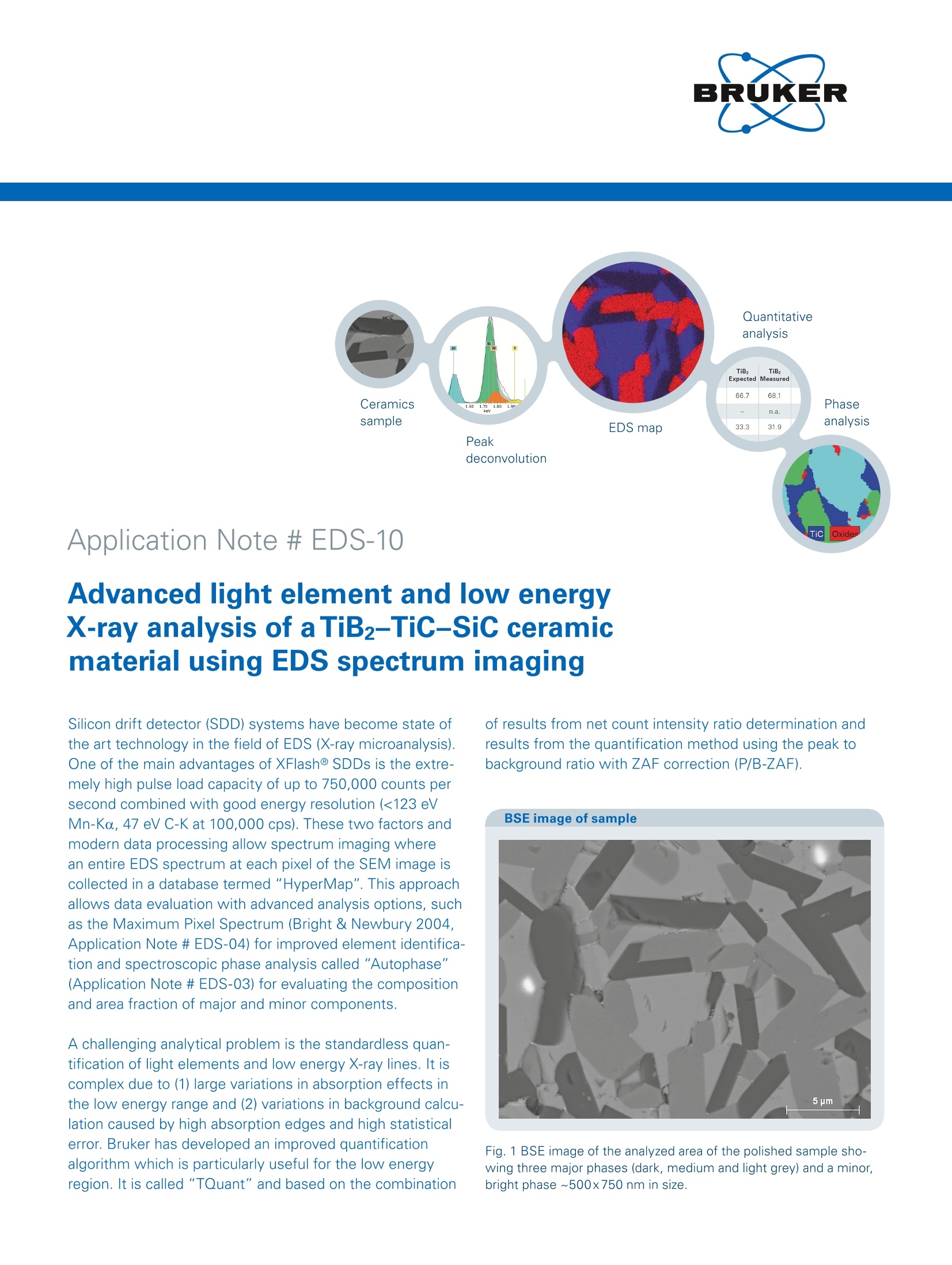
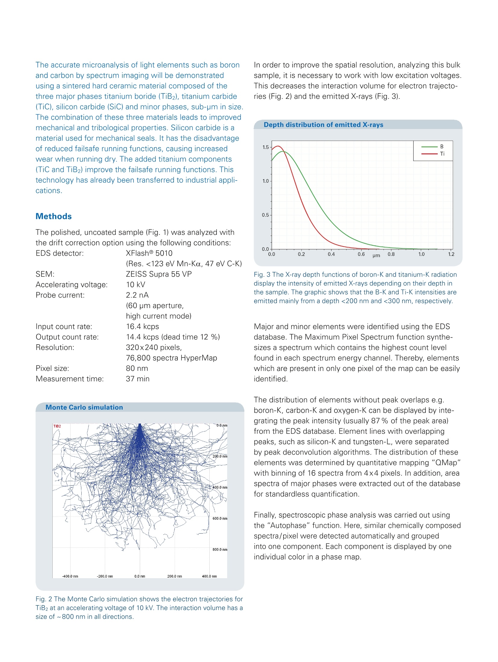
Ceramicssample Application Note # EDS-10 TiCOxideles Advanced light element and low energyX-ray analysis of a TiB2-TiC-SiC ceramicmaterial using EDS spectrum imaging Silicon drift detector (SDD) systems have become state ofthe art technology in the field of EDS (X-ray microanalysis).One of the main advantages of XFlash@ SDDs is the extre-mely high pulse load capacity of up to 750,000 counts persecond combined with good energy resolution (<123 eVMn-Ka, 47 eV C-K at 100,000 cps). These two factors andmodern data processing allow spectrum imaging wherean entire EDS spectrum at each pixel of the SEM image iscollected in a database termed"HyperMap". This approachallows data evaluation with advanced analysis options, suchas the Maximum Pixel Spectrum (Bright & Newbury 2004,Application Note # EDS-04) for improved element identifica-tion and spectroscopic phase analysis called "Autophase"(Application Note # EDS-03) for evaluating the compositionand area fraction of major and minor components. A challenging analytical problem is the standardless quan-tification of light elements and low energy X-ray lines. It iscomplex due to (1) large variations in absorption effects inthe low energy range and (2) variations in background calcu-lation caused by high absorption edges and high statisticalerror. Bruker has developed an improved quantificationalgorithm which is particularly useful for the low energyregion. It is called "TQuant" and based on the combination of results from net count intensity ratio determination andresults from the quantification method using the peak tobackground ratio with ZAF correction (P/B-ZAF). BSE image of sample Fig. 1 BSE image of the analyzed area of the polished sample sho-wing three major phases (dark, medium and light grey) and a minor,bright phase~500x750 nm in size. The accurate microanalysis of light elements such as boronand carbon by spectrum imaging will be demonstratedusing a sintered hard ceramic material composed of thethree major phases titanium boride (TiB2), titanium carbide(TiC), silicon carbide (SiC) and minor phases, sub-um in size.The combination of these three materials leads to improvedmechanical and tribological properties.Silicon carbide is amaterial used for mechanical seals. It has the disadvantageof reduced failsafe running functions, causing increasedwear when running dry. The added titanium components(TiC and TiB2) improve the failsafe running functions. Thistechnology has already been transferred to industrial appli-cations. Methods The polished, uncoated sample (Fig. 1) was analyzed withthe drift correction option using the following conditions: Monte Carlo simulation In order to improve the spatial resolution, analyzing this bulksample, it is necessary to work with low excitation voltages.This decreases the interaction volume for electron trajecto-ries (Fig. 2) and the emitted X-rays (Fig. 3). Fig. 3 The X-ray depth functions of boron-K and titanium-K radiationdisplay the intensity of emitted X-rays depending on their depth inthe sample. The graphic shows that the B-K and Ti-K intensities areemitted mainly from a depth <200 nm and <300 nm, respectively. Major and minor elements were identified using the EDSdatabase. The Maximum Pixel Spectrum function synthe-sizes a spectrum which contains the highest count levelfound in each spectrum energy channel. Thereby, elementswhich are present in only one pixel of the map can be easilyidentified. The distribution of elements without peak overlaps e.g.boron-K, carbon-K and oxygen-K can be displayed by inte-grating the peak intensity (usually 87% of the peak area)from the EDS database. Element lines with overlappingpeaks, such as silicon-K and tungsten-L, were separatedby peak deconvolution algorithms. The distribution of theseelements was determined by quantitative mapping“QMap"with binning of 16 spectra from 4x4 pixels. In addition, areaspectra of major phases were extracted out of the databasefor standardless quantification. Finally, spectroscopic phase analysis was carried out usingthe "Autophase" function.Here, similar chemically composedspectra/pixel were detected automatically and groupedinto one component. Each component is displayed by oneindividual color in a phase map. Identification Major elements such as boron, carbon, silicon and titaniumcan be easily detected in the sum spectrum of the complete analyzed area (Fig. 4a). The Maximum Pixel Spectrumreveals the presence of additional minor elements suchas aluminum and oxygen. The deconvolution result of theMaximum Pixel Spectrum clearly indicates the presence ofyttrium and tungsten (Figs. 4b-d). Fig. 4(a): Comparison of the sum spectrum (blue) of the analyzed area and the Maximum Pixel Spectrum (red). Elements which are presentonly in a few pixels of the map cannot be displayed in the sum spectrum due to the low overall concentration but are clearly identifiable in theMaximum Pixel Spectrum. (b-d): Deconvolution result of the Maximum Pixel Spectrum with considerations of different elements (coloredpeaks). Deconvolution with aluminum and silicon only (b) shows a mismatch in the range of 1.8-2.0 keV and at 1.35 keV when comparedto the background corrected Maximum Pixel Spectrum (black line). This indicates that not all element X-ray lines were correctly identified.The result with consideration of additional yttrium (c) fills the gap in the range of 1.9-2.0 keV. With consideration of additional tungsten (d),the grey area which is the sum of each deconvolved element matches the Maximum Pixel Spectrum in the range of 1.8-1.9 keV and alsoat 1.35 keV. The remaining small deviation at ~1.85 keV of the deconvolution result when compared to the Maximum Pixel Spectrum canbe explained due to the fact that the Maximum Pixel Spectrum is not a normal area spectrum but synthesized from channel intensities ofdifferent pixels. Here, the intensity is not a true combination of both elements Si and W as these are not really present in the same pixel.Thus, the amount of W is underestimated in the deconvolution result producing the described deviation. Peak intensity and quantitative element mapping Integrated peak intensity maps display the distribution ofthe major constituents boron and carbon (Fig.5a) as well asthe enrichment of aluminum and yttrium as oxides at grainboundaries (Figs. 5b-d). The quantitative map (Fig. 6) showsthe concentration of each element in false colors: Boron(Fig. 6a) is displayed by an orange color corresponding to 66.7 at.% (TiB2), carbon (Fig.6b) as well as silicon (Fig. 6c)appear in green color (50.0 at.%; TiC, SiC). The differentstoichiometry for titanium (33.3 at.% in TiB2and 50.0 at.%in TiC) can be distinguished by their blue and green color(Fig.6d). Tungsten-enriched inclusions (Fig. 6e) can beobserved within titanium carbide. The accurate distinction oftungsten and silicon demonstrates the accuracy of the peakdeconvolution model. Fig.5 Peak intensity maps of elements without peak overlaps. (a) Boron-K(red) and carbon-K (blue) are displayed as composite elementmaps. (b) Oxygen-K distribution shown in false color display overlaid with the BSE image, (c) aluminum-K and (d) yttrium-L. To avoid thatthe yttrium distribution is falsified by the overlap with the tungsten peak, a smaller peak area was used to display the yttrium intensity. The Quantitative maps of major constituents (e) Fig. 6 Quantitative maps (at.%) of (a) boron, (b) carbon, (c) silicon, (d) titanium and (e) tungsten. Major phases are easily identifiable by compa-ring concentrations in the same regions in different quantitative maps -TiB2, SiC and TiC have been labeled accordingly for easy reference. Standardless quantification of area spectra The mean values (Table 1) of representative areas consistingof 16 pixels (Fig. 7) for major phases are in good agreementwith the expected stoichiometry. When compared to expec- ted values, the deviation of the quantification result is <5 %.It has to be noted that 16 pixels of the map correspond to anintegration time of only <0.5 sec and an impulse statistics of5000-9000 counts in the complete spectrum. Table 1 Expected, stoichiometric values (at.%) of major phases are compared to quantification results. Mean values and standard deviationswere obtained by results of five different locations per phase, as shown in Fig. 7. The relative deviation is the difference between the quanti-fication result and the expected,stoichiometric value. N.a. - not analyzed, n.d. - not detected. TiB2 Expected TiB2 Measured /±at.% Deviation TiC TiCMeasured /±at.% Deviation/% SiC Expected SiC 卜Measured /±at.% Deviation/% /% Expected B 66.7 68.1 0.7 2.1 - n.d. - 一 n.d. - - n.a. 一- 50 49.8 1.2 -0.4 50 50.9 1.1 1.8 Ti 33.3 31.9 0.7 -4.2 50 50.2 1.2 0.4 n.d. 一 Si n.d - n.d. 一 50 49.1 1.1 -1.8 Measurement locations for quantitative analysis of major phases Fig. 7 Areas of major phases(4x4pixels) where spectra were extracted and quantified (Table 1). Spectroscopic phase analysis Chemically different components are shown in individuacolors in the phasemap (Fig.8). Phase spectra clearlydisplay the elements present in the major and minor phases (Fig.9). The area fraction of each phase is shown in(Table 2). Yttrium aluminum oxides make up to 2.3 %, thetungsten carbide phase 0.3 % of the whole area. l Fig. 8 Map showing the distribution of major and minor phases. Table 2 Area fraction of major and minor phases. Conclusion This analysis has demonstrated that state-of-the-art hard-ware in combination with modern data processing allowsadvanced spectral imaging also of light elements and lowenergy X-ray lines. Due to the unmatched light elementperformance of the XFlash@SD detector, the distribution ofelements such as boron and carbon can be easily revealedby peak intensity maps. Element identification can be significantly improved by theMaximum Pixel Spectrum. This function allows indentifyingelements which are present in only a few pixels of the map.Peak deconvolution is a powerful tool for identification anddiscrimination of elements with overlapping lines (e.g. Si-K,W-L). The distribution of these elements can be shown inquantitative maps. Phases Area fraction/% Area fraction/pixels Area fraction/pm² SiC 33.1 25,404 162 TiB2 32.4 24,889 159 TiC 31.9 24,490 157 Oxides 2.3 1,792 11 WC 0.3 225 1 Total 100.0 76,800 489 Even with low impulse statistics, area compositions oflight elements can be accurately quantified. The impulsestatistics of spectra can be improved by summing similarlycomposed areas using the "Autophase"function. Literature Bright, D.S. and Newbury, D.E. (2004). Maximum pixel spectrum:a new tool for detecting and recovering rare, unanticipated featuresfrom spectrum image data cubes, Journal of Microscopy, Vol. 216,Issue 2, pp. 186-193. Author Dr. Tobias Salge, Application Scientist EDS, Bruker Nano GmbH Acknowledgements The author would like to thank Dr. Rolf Wasche and Dr. DanHodoroaba (BAM) for the hard material ceramics and Dr. MathiasProcop (lfG) for a stimulating discussion. Bruker Nano GmbH Berlin· Germany Phone +49 (30) 670990-0 Fax +49 (30)670990-30 info.bna@bruker.com www.bruker.com/quantax-eds-for-sem This analysis has demonstrated that state-of-the-art hardwarein combination with modern data processing allowsadvanced spectral imaging also of light elements and lowenergy X-ray lines. Due to the unmatched light elementperformance of the XFlash® SD detector, the distribution ofelements such as boron and carbon can be easily revealedby peak intensity maps.Element identification can be significantly improved by theMaximum Pixel Spectrum. This function allows indentifyingelements which are present in only a few pixels of the map.Peak deconvolution is a powerful tool for identification anddiscrimination of elements with overlapping lines (e.g. Si-K,W-L). The distribution of these elements can be shown inquantitative maps.Even with low impulse statistics, area compositions oflight elements can be accurately quantified. The impulsestatistics of spectra can be improved by summing similarlycomposed areas using the “Autophase” function.
关闭-
1/8
-
2/8
还剩6页未读,是否继续阅读?
继续免费阅读全文产品配置单
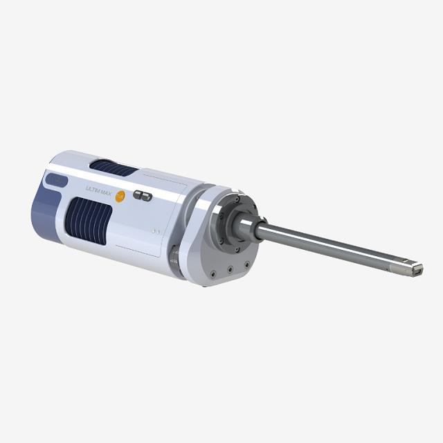
布鲁克电子显微纳米分析仪器部为您提供《TiB2 – TiC – SiC中元素检测方案(X射线能谱仪)》,该方案主要用于涂料中含量分析检测,参考标准《暂无》,《TiB2 – TiC – SiC中元素检测方案(X射线能谱仪)》用到的仪器有布鲁克 , EDS, 能谱仪, SEM, TEM、布鲁克 QUANTAX EDS 能谱仪(TEM)、布鲁克3D EDS/EBSD重构软件QUBE。
我要纠错
推荐专场
相关方案
 咨询
咨询