

方案详情文
智能文字提取功能测试中
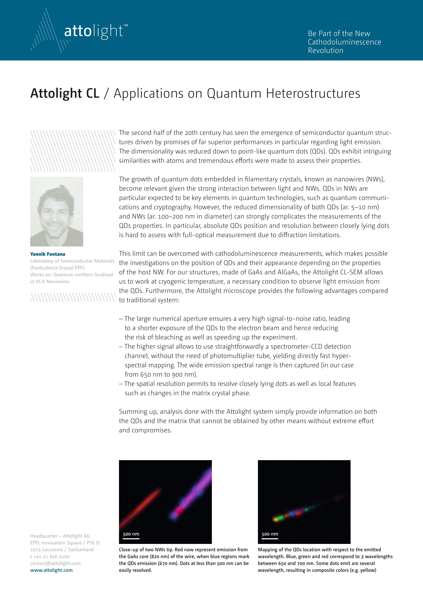
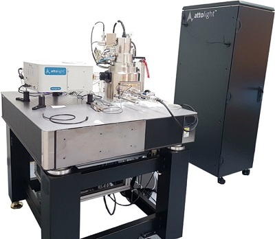
阴极荧光分析设备SEM-CL在量子点异质结方面的应用attolightBe Part of the NewCathodoluminescenceRevolution Attolight CL / Applications on Quantum Heterostructures The second hal f of the 2oth century ha s seen the emergence of semiconductor quantum struc-tures driv e n by promises of far s u perior performances in particular reg a rding l ight emission.The dimensionality was reduced down to point -like quantum d o ts (QDs). QDs exhibit intriguing similari t ies with atoms and tremendous efforts were made to assess thei r propert i es The growth of quantum dots e mbedded i n filamentary crystals, known as nanowires (NWs),become relevant g i ven the strong interac t ion between light and NWs. QDs in NWs are par t icular expected to be key e l ements in quantum tech n ologies, such as quantum commun i -cations and c r yptography. However , the reduced dimensionality of both QDs (ar. 5-10 nm)and NWs (ar. 100-200 nm i n diameter) can strongly complicates the measurements of the QDs propertie s . In particular, absolute QD s position and resol u tion between closely lying dots i s hard to assess with full-optical measurement due to dif f rac ti on l imitations. Y an nik F o nt a n a Laboratory of Semiconductor Materials (Fontcuberta Grou p) E PFL Works on: Quantum emitters localized in III-V Nanowires This limit can be overcomed with cathodoluminescence measurements, which makes possible t he investigations on the position of QDs an d the i r appea r ance depending on t he propert i es o f the hos t NW. For our structures, made of GaAs a n d AlG a As, the Attol i ght CL-SEM allows us to work at cryogenic temperature, a necessary condi t ion to observe light emission from the Q D s. Furthermore , t he Attol i ght micro s cope provides the following advantages comp a red to traditional system: - The large numerical aperture ensures a very high signal -to -noise ratio, lead i ng to a shorter exposure of the QDs to t he electron beam and hence red u cing the risk of bleaching a s well a s speed i ng up the experiment. - The h i gher signal allows to use straightforwardly a spec t rometer-CCD detec ti on channel, wit h out the need of photomu l t i pl i er tube, y i elding di r ec t ly fas t hyper -spectral mapping. The wide em i ssion spectral r a nge i s then c a ptured (in our case trom 650 nm to 900 nm). - The spatial resolut i on permits to resolve closely lying dots as wel l as local features such as changes i n the matrix crystal phase. Summing up, an a lysi s done with the Attolight system simply provide i nformation on both the QDs a n d the matr i x that cannot be obta i ned by other means without extreme effort and compromises. 500 nm 500 nm Close-up of two NWs tip. Red now represent emission from the GaAs core (820 nm) o f the wire, when blue regions mark the QDs emission (670 nm). Dots a t l ess than 500 nm can be easily resolved. Mapping of the QDs location with respect to the emitted wavelength. Blue, green and red correspond to 3 wavelengths between 650 and 7o0 nm. Some dots emit are several wavelength, resul t i ng i n composite colors (e.g. yellow)
关闭-
1/1
产品配置单
北京正通远恒科技有限公司为您提供《SEM-CL在量子点异质结方面的应用》,该方案主要用于其他中阴极荧光分析设备检测,参考标准《暂无》,《SEM-CL在量子点异质结方面的应用》用到的仪器有快速定量阴极发光CL-SEM系统 Allalin。
我要纠错
推荐专场
半导体器件测试仪器
更多
相关方案
 咨询
咨询