

方案详情文
智能文字提取功能测试中
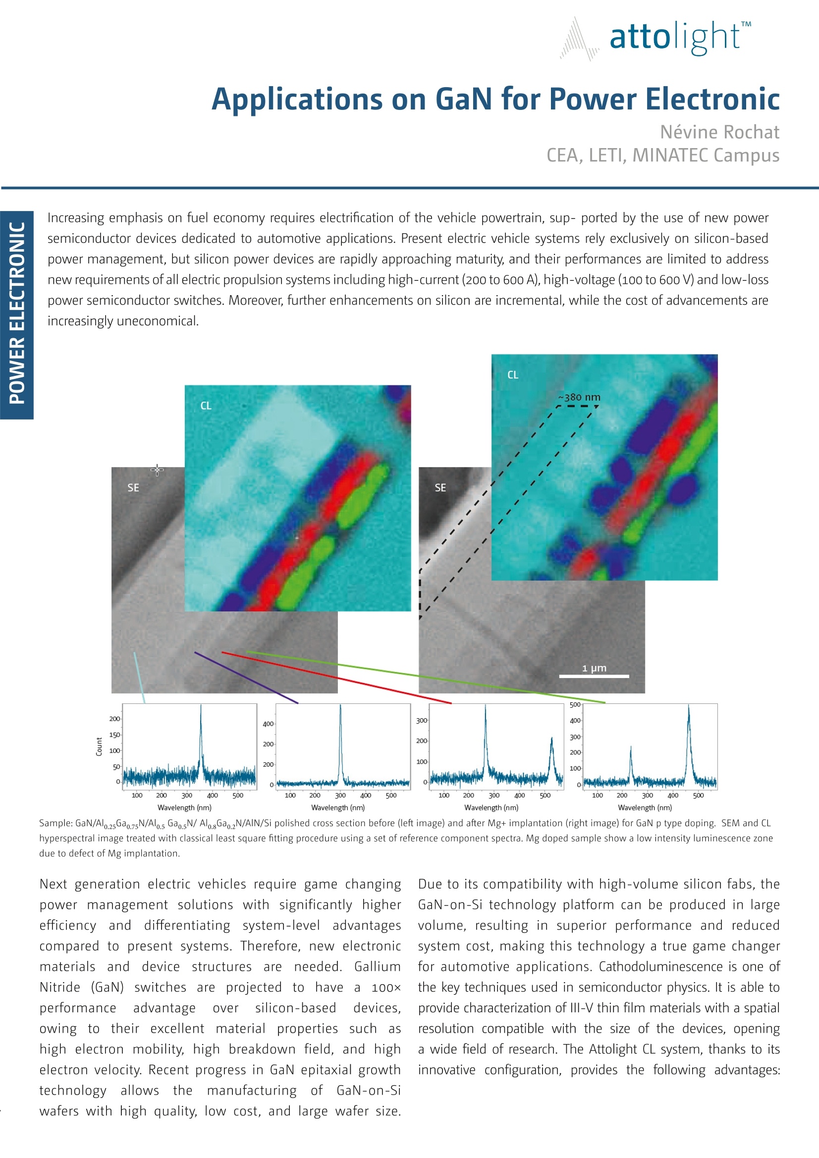
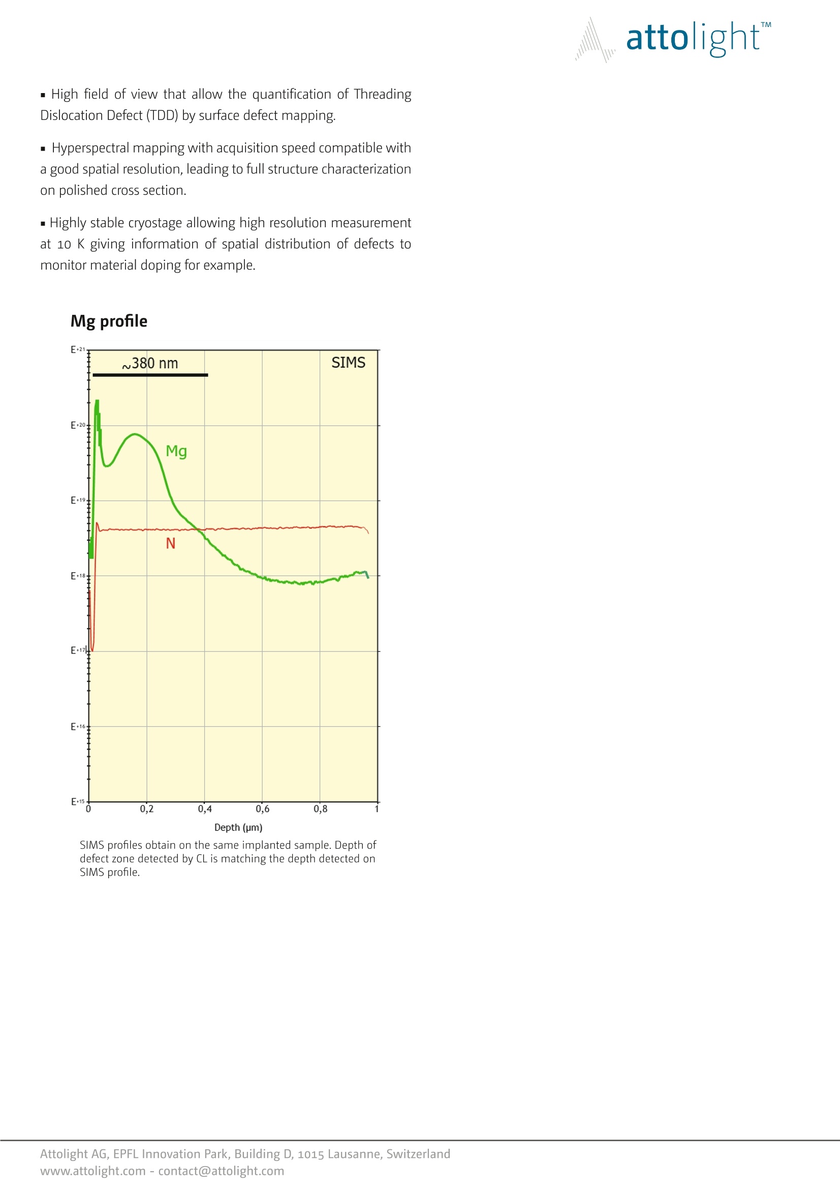
对燃油经济性的日益重视要求车辆动力系统电气化,并由新动力的使用提供支持专用于汽车应用的半导体器件。目前的电动汽车系统完全依赖于硅基材料电源,但硅功率器件正迅速接近成熟,其性能有限,这对解决所有电力推进系统提出了新的要求,包括大电流(200至600 A)、高电压(100至600 V)和低损耗功率半导体开关。此外,硅的进一步增强是增量的,而花费的成本却越来越不合算。图一:样品:GaN/Al0.25Ga0.75N/Al0.5 Ga0.5N/ Al0.8Ga0.2N/AlN/Si为GaN p型掺杂前(左图)和注入Mg+后(右图)的抛光截面。 与现在的系统相比,下一代电动汽车需要改变游戏规则:电源需体现出更高效率和差异化的系统级优势。因此,新电子需要材料和器件结构。氮化镓(GaN)开关预计具有100x优于硅基器件的性能优势,由于其优异的材料性能,如:高电子迁移率,高击穿场,高电子速度。GaN外延生长的最新进展技术允许制造GaN-on-Si高品质、低成本、大晶圆尺寸的晶圆。 由于其与大批量硅晶圆厂的兼容性,GaN-on-Si技术平台可以大规模生产体积大且性能优越的硅晶圆而减小成本,使这项技术真正改变了游戏规则并用于汽车领域。阴极发光是其中半导体物理中使用的关键技术。它能够提供III-V薄膜材料的空间表征分辨率从而开辟出广阔的研究领域。 Attolight CL系统,由于它的创新配置,可以应用在以上半导体物理研究中并提供以下优势:1、高视场,可量化穿线位错缺陷(TDD)的表面缺陷映射。2、高光谱制图与采集速度兼容良好的空间分辨率,导致完整的结构表征在抛光截面上。3、高度稳定的冷冻阶段允许高分辨率测量在10k时给出缺陷的空间分布信息例如,监测材料掺杂。图二:在同一植入样品上获得SIMS剖面。CL检测到的缺陷区域深度与SIMS剖面检测到的深度相匹配。Applications on GaN for Power Electronic Névine Rochat CEA, LETI, MINATEC Campus Increasing emphasis on fuel economy requires electrifciation of the vehicle powertrain, sup- ported by the use of new power semiconductor devices dedicated to automotive applications. Present electric vehicle systems rely exclusively on silicon-based power management, but silicon power devices are rapidly approaching maturity, and their performances are limited to address new requirements of all electric propulsion systems including high-current (200 to 600 A), high-voltage (100 to 600 V) and low-loss power semiconductor switches. Moreover, further enhancements on silicon are incremental, while the cost of advancements are increasingly uneconomical. Sample: GaN/Al 0.25Ga 0.75N/Al 0.5 Ga 0.5N/ Al 0.8Ga 0.2N/AlN/Si polished cross section before (lef timage) and afetr Mg+ implantation (right image) for GaN p type doping. SEM and CL hyperspectral image treated with classical least square ftiting procedure using a set of reference component spectra. Mg doped sample show a low intensity luminescence zone due to defect of Mg implantation. Next generation electric vehicles require game changing power managementsolutions with significantlyhigher efficiency and differentiating system-level advantages comparedtopresentsystems.Therefore,newelectronic materials and device structures are needed. Gallium Nitride (GaN) switches are projected to have a 100×performance advantage over silicon-based devices, owing to their excellent material properties such as highelectronmobility,highbreakdownfield,andhigh electron velocity. Recent progress in GaN epitaxial growth technology allows the manufacturing of GaN-on-Si wafers with high quality, low cost, and large wafer size. Due to its compatibility with high-volume silicon fabs, the GaN-on-Si technology platform can be produced in large volume,resultinginsuperiorperformanceandreduced system cost, making this technology a true game changer for automotive applications. Cathodoluminescence is one of the key techniques used in semiconductor physics. It is able to provide characterization of III-V thin film materials with a spatial resolutioncompatiblewiththesizeofthedevices,opening a wide field of research. The Attolight CL system, thanks to its innovativeconfiguration,providesthefollowingadvantages: · High field of view that allow the quantification of Threading Dislocation Defect (TDD) by surface defect mapping. · Hyperspectral mapping with acquisition speed compatible with a good spatial resolution, leading to full structure characterization on polished cross section. ▪ Highly stable cryostage allowing high resolution measurement at 10 K giving information of spatial distribution of defects to monitor material doping for example. Mg proflie SIMS proflies obtain on the same implanted sample. Depth of defect zone detected by CL is matching the depth detected on SIMS proflie.
关闭-
1/2
-
2/2
产品配置单
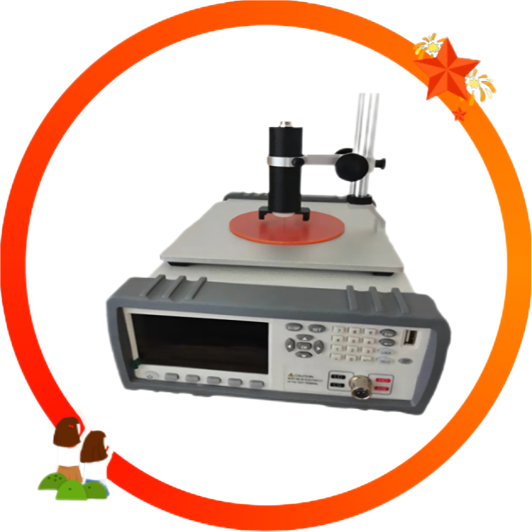
北京正通远恒科技有限公司为您提供《阴极发光设备(SEM-CL)在GaN功率电子方面的应用》,该方案主要用于其他中GaN功率电子检测,参考标准《暂无》,《阴极发光设备(SEM-CL)在GaN功率电子方面的应用》用到的仪器有快速定量阴极发光CL-SEM系统 Allalin。
我要纠错
推荐专场
半导体器件测试仪器
更多
相关方案
 咨询
咨询