方案摘要
方案下载| 应用领域 | 半导体 |
| 检测样本 | 其他 |
| 检测项目 | |
| 参考标准 | 无 |
Development and testing of semiconductor devices requires extensive knowledge of local structure and elemental composition. With feature sizes of <5 nm, it is often necessary to perform imaging and EDS analysis in a S / TEM. Once in the TEM, there are still many difficulties to be overcome to acquire accurate elemental maps. Elemental analysis of semiconductors is typically difficult due to strong overlaps of X-ray lines between commonly used elements and low concentrations of dopants. Not only are concentrations of dopants small but their X-ray lines often overlap with other materials used in semiconductor processing. This brief shows how AZtecTEM solves these overlaps to achieve an accurate elemental analysis. TEM Semiconductor Mapping in the TEM Solving peak overlaps in real-time Application Brief

Development and testing of semiconductor devices requires extensive knowledge of local structure and elemental
composition. With feature sizes of <5 nm, it is often necessary to perform imaging and EDS analysis in a S / TEM.
Once in the TEM, there are still many difficulties to be overcome to acquire accurate elemental maps. Elemental
analysis of semiconductors is typically difficult due to strong overlaps of X-ray lines between commonly used elements
and low concentrations of dopants. Not only are concentrations of dopants small but their X-ray lines often overlap
with other materials used in semiconductor processing. This brief shows how AZtecTEM solves these overlaps to
achieve an accurate elemental analysis.
TEM Semiconductor Mapping in the TEM
Solving peak overlaps in real-time
Application Brief
文献贡献者


一文了解 EDS 能谱技术发展历程
应用分享|红外辐射全无惧——牛津仪器新型高温 EDS / EBSD 助力原位分析

AZtecBattery 在锂离子电池清洁度检测中的应用
相关产品
牛津EMCCD探测器iXon Ultra 897
牛津EMCCD探测器iXon 888
日本电子JED能谱元素分析系统 AZtecTEM
透射电镜元素分析系统 牛津仪器能谱仪Xplore TEM
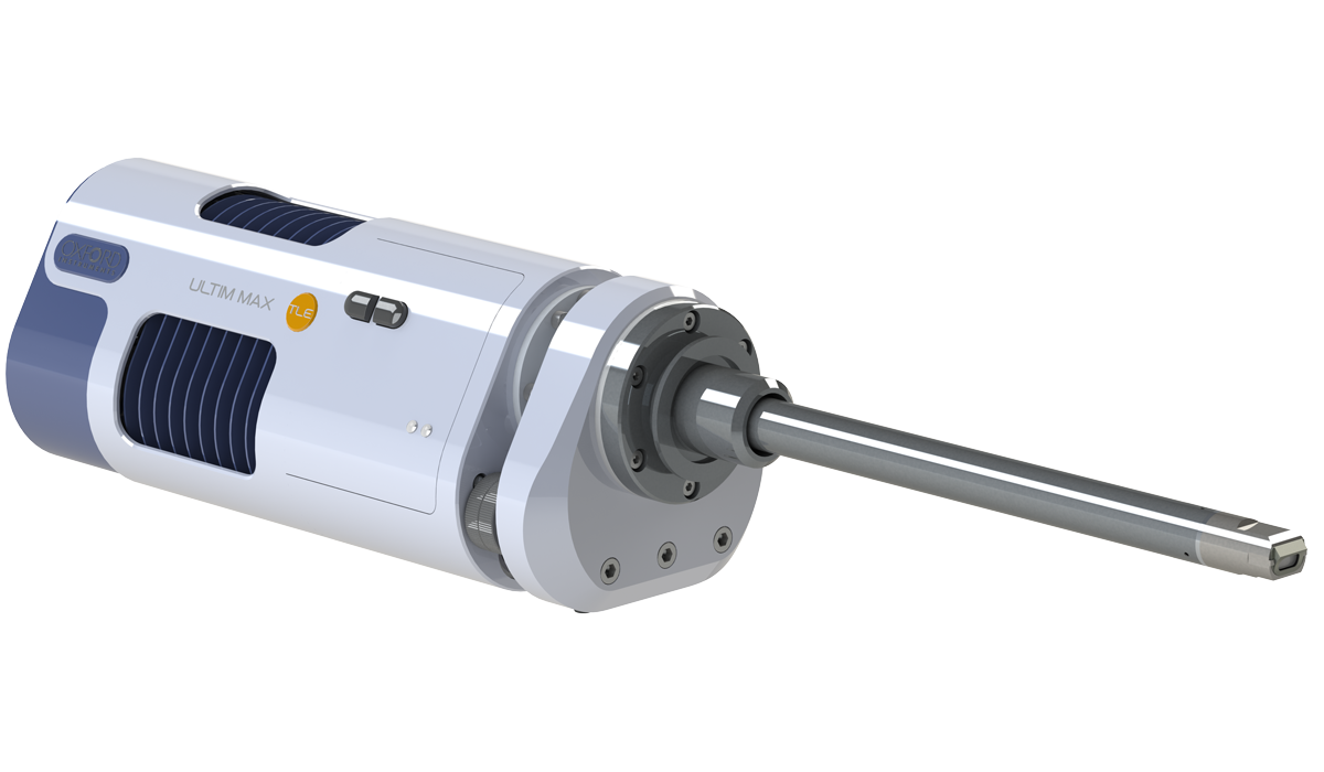
透射电镜元素分析系统 牛津仪器能谱仪UltimMax TLE
透射电镜元素分析系统 牛津仪器能谱仪UltimMax TEM
台式共聚焦显微镜BC43牛津仪器ANDOR
牛津仪器原子力显微镜 Cypher VRS1250
扫描电镜微量元素分析系统 牛津仪器波谱仪AZtecWave
Sona sCMOS 生命科学显微相机平台
用于天文学和物理科学的超灵敏背照式sCMOS相机
波长色散谱仪
电镜专用微区结构分析---牛津仪器全能型 S2 EBSD
牛津仪器Proteox5mK 稀释制冷机
牛津仪器快速扫描电容显微镜(SCM)

关注

拨打电话

留言咨询