方案摘要
方案下载| 应用领域 | 半导体 |
| 检测样本 | 其他 |
| 检测项目 | |
| 参考标准 | 暂无 |
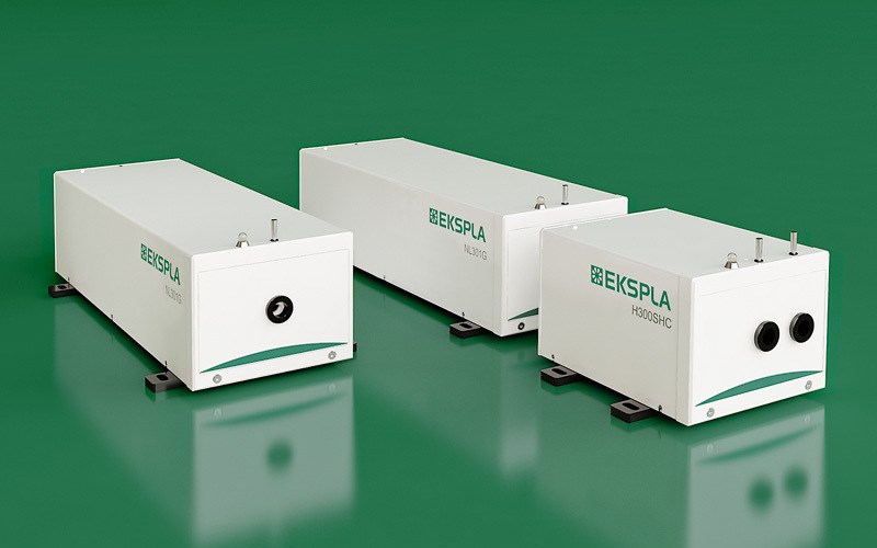
采用立陶宛Ekspla公司的NL303G型激光器的基频1064nm,10Hz输出重复频率,利用分光技术分成两束,然后在一个2X2平方毫米的区域内形成强度周期性变化的干涉条纹,并利用这一光束进行不定形硅的结晶化处理。
Laser crystallization of a 50‐nm thick amorphous‐Si (a‐Si) thin film on glass substrate was examined by a Nd:YAG (λ = 1064 nm) nanosecond laser and a two‐beam laser interference method. In spite of the low absorption rate of the laser wavelength in the a‐Si, crystallized Si ripple patterns were observed following a single laser pulse irradiation. The atomic force microscope (AFM) measurement revealed that surface ripple arrays are protruded as high as
120 nm at the positions corresponding to the maximum laser intensity and the ripples are composed of narrow double peaks with a separation of 1 μm.Raman image mapping was used to plot the spatial distribution of the crystallized Si phase. It was found that a 1064‐nm‐wavelength nanosecond laser could crystallize an a‐Si thin film into polycrystalline‐Si (poly‐Si) by nonlinear absorption under high laser energy irradiation.
文献贡献者


在一个双稳湍流涡旋火焰中,对间歇性动态的时间-频率定位
Particle-laden Taylor-Couette流:高阶转变和径向局部波浪涡旋的证据

7根杆束的流体-结构相互作用:用实验数据对比数值模拟
相关产品
汽车光学检测系统AIS
PT403型波长可调谐皮秒激光器
ANL系列高能量高重复频率DPSS纳秒激光器
APL4206 系列高能量皮秒激光放大器
UltraFlux FF/FT 5000 高能量可调谐飞秒激光器系统
UltraFlux FT300型波长可调谐飞秒激光器系统
Ekspla 超高功率激光器系统SYLOS 2A
LaVision PTUx 可编程时间控制单元
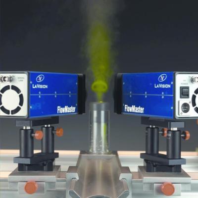
LaVision 用于粒子成像测速PIV的相机
LaVision StrainMaser 全场应变测试系统组件
LaVision 用于数字图像相关DIC的相机
LaVision StrainMaster 数字图像相关分析软件包
LaVision 标定板
LaVision StrainMaster 形变应变成像测量系统
LaVision StrainMaster DVC 体视全场应变测量系统

关注

拨打电话

留言咨询