

 仪器对比
仪器对比


 关注
关注
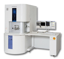
Hitachi's high performance FIB-SEM provides unparalleled nano-analyses of devices and functional materials !!
Legendary Hitachi reliability and performance in an integrated system (Ultra-high performance FIB and high resolution FE-SEM) enabling high-throughput specimen preparation, high resolution imaging and analysis and precision nanofabrication. New low-damage fabrication techniques have been developed for materials sensitive to electron irradiation. Innovations in sample loading, sample navigation, and Micro-sampling increase analysis efficiency(*1).
Features |
Ultra-high performance FIB
- Low CsFIB optics(*2) deliver 50nA or more of beam current (@40kV) in an about 1µm spot-size. The high current enables unconventional large-area milling, hard material fabrication and high throughput multiple specimen preparation.
New Micro-sampling
- Hitachi's patented Micro-sampling technology provides smooth probe motion. Also, the probe can be used for newly developed absorbed current imaging(*1) to aid fault isolation.
High precision end-point detection
- High resolution SEM allows high precision end-point detection. Section-view function, which displays an outline of the cross-section utilizing the real-time FIB image, is ideal for preparing electron irradiation sensitive specimens like low-K material.
High resolution SEM
- Hitachi's unparalleled SEM column and detector design(*2) enables high resolution SEM imaging during and after FIB fabrication.
Holder compatibility with TEM/STEM(*1)(*2)
- A side entry STEM/TEM-type staqe(*1) allows the use of the same specimen holder (compatible with NB5000 and Hitachi TEM/STEM). No tweezer handling of specimen during transfer results in higher throughput TEM/STEM analysis.
(*1):Optional accessory
(*2):Hitachi patent
Low Cs FIB optics: patent pending, Micro-sampling: JP2774884/US5270552, Section-view function: patent pending, SEM column and detector design: JP3081393/US5387793, Holder compatibility: JP2842083
Specifications
| FIB | Accelerating voltage | 1 - 40kV | |
| Beam current | 50 nA or more @ 40kV (CP) | ||
| SIM resolution | 5nm @ 40kV (CP) | ||
| Magnification | ×60 - ×250,000 | ||
| Ion source | Ga Liquid Metal Ion Source | ||
| Lens system | Low Cs 2-stage electrostatic lens system | ||
| SEM | Accelerating voltage | 0.5 - 30kV | |
| SEM resolution | 1.0nm @ 15kV (CP) | ||
| Magnification | High Mag mode | ×250 - ×800,000 | |
| Low Mag mode | ×70 - ×2,000 | ||
| Electron source | ZrO/W Schottky emission | ||
| Lens system | 3-stage electromagnetic lens reduction system | ||
| Signal selection | SEM | Upper SE, Lower SE, Absorbed current(*1) | |
| FIB | Lower SE, Absorbed current(*1) | ||
| Eucentric stage | Traverse range |
X: 50mm (30mm(*2)), Y: 50mm (30mm(*2)), Z: 22mm |
|
| T: -1.5 - 58.3°, R: 360° | |||
| Sample size | Maximum diameter | Φ50mm (Φ30mm(*2)) | |
| Deposition | Material | Tungsten/Carbon (changeable) | |
| Micro-sampling | Probe exchange | Load lock type | |
| Additional function | Touch sensing, Absorbed current imaging(*1) | ||
CP:Beam Cross Point
(*1):Optional accessory
(*2):When side entry stage is ordered
-
NX2000(FIB-SEM-Ar)三束在单晶铁与单晶硅透射电镜样品制备中的应用
半导体 2019-05-30


- 相关仪器


相关产品

