
方案详情文
智能文字提取功能测试中
Film Metrology SpecialistsFor further information please contact us at info@thetametrisis.com or sales@thetametrisis.comThetaMetrisis S.A. O 2009, www.thetametrisis.com ThetaMetrisis APPLICATION NOTE #001 Characterization of Si membranesUsing White Light Reflectance Spectroscopy (WLRS) Goal: The characterization of thin Si membranes. Means & Methods: Samples were suspended Si membranes on Si wafers with intermediate layers of SiO2. Siabsorbs in the visible range of the spectrum and for thick membranes measurements should be performed inthe NIR range. The measurements performed with an FR-Basic IR operating in the 900-1700nm spectral range.The reflection probe used in the present evaluation has an optical reflectance diameter of ~500X500um. Results: In fig. 1, a representative reflectance spectrum for the 900-1700nm range from a Si membrane isillustrated. The membrane area is 300X900um. The stack considered in this case was Air/Si(100)/SiOz/Air i.e. asuspended Si membrane on an ultra thin SiO2 layer, fabricated with back-side etching of the supporting Siwafer. In fig. 2 a blow-up in the spectral region (930-1200 nm) used for the fitting is shown. The calculated filmSi membrane thickness is 5.25um. Figure 2: Experimental and fitted reflectance spectrafor fig's 1 data. In fig. 3 the experimental and fitted reflectance spectrum from a SOl wafer are shown. The cavity is300X900um. The calculated thicknesses for the Si over layer and the SiO layer are 5.04um and 0.48um respectively. Figure 3: Reflectance and fitted spectrum from a SOl wafer. Conclusions WLRS methodology is capable of measuring the filmthickness of Si membranes over a wide thicknessrange starting from few tens of nm up to severalmicrons (depending on the Fr-Basic configuration). KOH etching produces surface etching that is toohigh for the WLRS methodology. In case of back-etchor front-etch Si cavities/membranes double-sidedwafers should be used. 显示了硅膜在900-1700nm范围内的反射光谱。膜面积为300x900μm2。在这种情况下,考虑的堆叠是空气/Si(100)/SiO2/空气,即超薄SiO2层上的悬浮Si膜,由支撑Si晶片的背面蚀刻制成。 显示了用于拟合的光谱区域(930-1200 nm)中的放大。计算得到的薄膜厚度为5.25μm。显示了SOI晶片的实验和拟合反射光谱。空腔为300x900μm2。Si覆盖层和SiO2层的计算厚度分别为5.04μm和0.48μm。WLRS方法能够测量从几十纳米到数微米(取决于fr的基本配置)的大厚度范围内的硅膜厚度。 KOH蚀刻产生的表面蚀刻对于WLRS方法来说太高了。如果是背面蚀刻或正面蚀刻,则应使用Si空腔/膜双面晶圆FR的工具基于白光反射光谱(Reports) 。准确同步的厚度测量及薄膜的折射率-一个广泛的多样化的应用范围广泛的光电特性的工具和整体解决方案,如:半导体、有机电子、聚合物、涂料和涂料、光伏、生物传感、化学传感...
关闭-
1/1

产品配置单
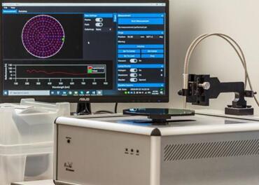
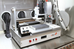
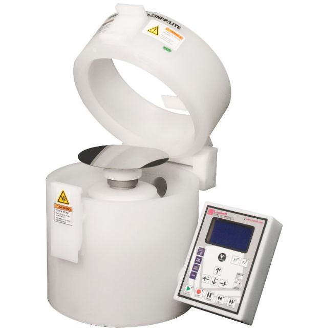
迈可诺技术有限公司为您提供《SiO2中Si膜表征检测方案(白光干涉测厚)》,该方案主要用于电子元器件产品中Si膜表征检测,参考标准《暂无》,《SiO2中Si膜表征检测方案(白光干涉测厚)》用到的仪器有扫描型光学膜厚仪 FR-Scanner、进口纳米狭缝涂布机、美国Laurell匀胶机WS-650-23NPPB。
我要纠错
推荐专场
相关方案
 咨询
咨询