

方案详情文
智能文字提取功能测试中
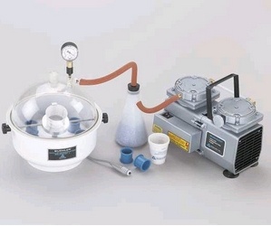
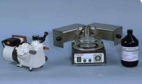
Published by BuehlerVolume 3, Issue 1 TECH-TIPSAn ITW Company TECH-NOTES USINGMICROSTRUCTURAL ANALYSIS TO SOLVE PRACTICAL PROBLEMS Microelectronics, Part I: Cutting, Mounting Introduction For most microelectronic devices and pack-ages, direct microscopic observation of across section is an important means of in-specting a particular defect. The creation ofa cross section, as a destructive measure,isoften used in the microelectronics lab as adecisive and final inspection tool after allother economical means of nondestructiveinspection are employed. In order to produce a cross section, many ofthe techniques used in the metals industryhave been borrowed; to a large degree, withsuccess. However, the philosophy and logicfor choosing a particular method of cutting,mounting, and abrasive preparation has of-ten been lost in the process. This is ofextreme significance because the needs ofthe microelectronics industry vary greatlyfrom those of the metals industry. Issues suchas feature size, specific area cross section-ing, and the ability to prepare a variety ofmaterials with different mechanical proper-ties within a single plane of polish requirean understanding of basic abrasive pro-cesses so that appropriate sectioningmethods might be developed. This issue of TECH-NOTES is the first half ofa two part effort to summarize some of thebasic concepts involved in proper prepara-tion of microelectronic materials. We willdiscuss some simple guidelines which themicroelectronic materials analyst might drawupon in the development of better prepara-tion techniques. In particular, this issue willcover the variables involved in cutting andmounting of microelectronic materials, andsummarize some of the technique and con-sumable choices that must be consideredin order to achieve quality results. The nextmicroelectronics issue of TECH-NOTES willcontinue with the abrasive processes ofgrinding and polishing these materials. Specimen Preparation Philosophy When considering preparation of a micro-electronic device and/or package, the firststep is to determine which materials arepresent in the cross section of interest. Thisis critical since these materials and theirmechanical properties will determine, to alarge degree, the course of action we take. Consider, for example, a small epoxy pack-age in which we desire to cross section asilicon die and a gold ball bond near thedie’s edge. If we were to encapsulate thepackage and grind to the edge of the die,(assuming the use of appropriate abrasivesand technique), we might produce satisfac-tory results in a reasonable period of time. This course of action would not be so easy,however, if the package were instead com-posed of ceramic. In this case, severalchoices present themselves. We can try togrind through the package, but we would, ofcourse, require an aggressive grinding me-dium which may annihilate the brittle siliconupon contact. In addition to destroying thematerials we plan to analyze, we would prob-ably spend an inordinate amount of time (notto mention expense) getting to this point. Abetter option is to cut the package near tothe plane of interest, using a precision dia-mond saw, and then to encapsulate thespecimen for subsequent preparation. Blade Purpose 15 HC, LC General purpose blades for sectioning 10 LC metals, ceramics, composites, etc. Ideal for sectioning packaged semi- conductors with mineral filled epoxy,glass-organic, or ceramic packages. 5 LC Ideal for sectioning bare die semi- conductors, and some ceramic-based packages The basic example above hints at a simplephilosophy of preparation in which we care-fully consider each stage of the process andit’s consequences towards the materials wechoose to analyze. The following text sum-marizes basic cutting and encapsulationprocesses in order to promote a logicalcourse of planning for microelectronic ma-terials preparation. Cutting a specimen close to the target planehas one major benefit, if performed prop-erly. It allows us to bypass much of thegrinding that consumes both abrasives andoperator time. This is especially true, as ex-plained previously, when ceramic packagingmaterials are present. The errors that are commonly associated with cuttingmicroelectronic devices have caused many to fear thismethod of specimen reduction as an alternative to grind-ing. However, if one is armed with some basic knowledgeof available blades, and some simple techniques to protectthe specimen, much wasted time and frustration can beavoided Table 1 describes the three series of metal-bonded dia-mond blades typically used for cutting microelectronicdevices. Decreasing number designations represent de-creasing abrasive size, while HC and LC represent highand low abrasive concentration. Typically, low abrasive con-centration is desired for sectioning hard, brittle materials,such as ceramics and semiconductors, due to the high loadper unit diamond required for reasonable cutting rates. Fig-ure 1 illustrates relative abrasive sizes for the three bladeslisted in Table 1. Figure 2 illustrates the surface finish andinduced damage produced by these blades. Although the finest abrasive produces the best surface fin-ish, there is a trade-off. Finer abrasives may, in some cases,significantly increase cutting times. This is especially truewhen polymeric packaging materials are involved. For pack-age applications, the 10LC series blades tend to givesatisfactory results in a reasonable period of time. While blade choice is extremely important in minimizingcutting damage, it is only half the battle. Other importantfactors for producing good results include choosing an ap-propriate lubricant/coolant, dressing the blade, andorienting the specimen in order to preserve the features ofinterest. Typically, the better a lubricant/coolant wets the specimenand the abrasive in the blade, the less blade‘loading’willoccur. Loading is the process by which ductile materials,such as copper, aluminum, or polymers, adhere to the con-stituents of the blade and decrease their cuttingeffectiveness. This type of loading may occur in a variety ofways. For instance, when the contact point between speci-men and blade is not well lubricated, friction creates highlocal temperatures. Such temperatures may result in local-ized welding or‘galling’between ductile metals and blade constituents. Many polymers, on the other hand, softenunder high temperature conditions, and adhere tenaciouslyto the edge of the blade, again reducing blade effective-ness. Hard materials, such as ceramics, can also produceloading, but through a completely different mechanism.They may cause the ductile binder material in the blade,itself, to smear over the abrasive, thus reducing the cuttingrate. For low-speed applications, the best results will beachieved by using a lubricant such as ISOCUT Fluid. Thisproduct provides extremely good surface wetting at lowspeeds, but it has a drawback for microelectronics applica-tions. It is an oil-based lubricant, which can be difficult tothoroughly clean from small recesses found in many mi-croelectronic devices. An alternative is ISOCUT PLUS Fluid.This water-based lubricant/coolant was designed for bothlow and high speed cutting, and provides excellent wettingproperties for nearly all applications. The fact that it is wa-ter-based makes it easier to rinse from the specimen aftercutting. Figure 3. ISOCUTand ISOCUT PLUS cutting fluids. ISOCUTPLUS should be diluted with water prior to use. Figure 4. Dressing of the blade should be performed beforeeach cut. Using a dressing stick holder (as shown in thefigure), instead of holding the stick by hand, prevents bladedamage. While an appropriate lubricant/coolant can reduce the ef-fects of loading, it would not eliminate them entirely. Dressingthe blade is also critically important and is often overlookedwhen cutting. Dressing involves cutting into a special abra-sive stick (the appropriate dressing stick is supplied witheach blade) to remove loaded material from the blade’scutting surface, seSe Figure 4. Typically,a single cut whichextends halfway through the dressing stick is sufficient todress the blade before each specimen cut. If cutting through Figure 2. Brightfield images representing cut surface finish produced in a microelectronic device by a) 15 series diamondwafering blade; b) 10 series blade; c) 5 series blade. a specimen which has previously been mounted in resin,dressing should be performed continuously during the cut-ting process to clean the resin material from the abrasivesurface of the blade. Figure 5. a) Orienting the specimen with longest dimensiontangent to the blade produces long cutting times. In addition,thin film coatings and substrate may be damaged. b) Orientingthe specimen with shortest dimension tangent to the bladedecreases cutting times. Thin film layers on trailing edge ofthe specimen are in tension and can be damaged or separated.c) Proper orientation is illustrated. Tilting the specimenminimizes vibration, and placing thin film layers at the leadingedge keeps them in compression against the substrate. Finally, and possibly most important of all, is the issue ofspecimen orientation during the cutting process. Brittle ma-terials such as silicon and ceramics are much stronger incompression than in tension, it is important to orient thespecimen so that the surface or interface of interest is putinto compression by the approaching abrasive. Figure 3illustrates the best orientation for a specimen in which thethin film circuitry must be preserved. It should be noted thatthe trailing edge of a brittle material, if unsupported by pack-aging, for instance, will be put in tension during cutting.Therefore, choices must sometimes be made about whichedge of the specimen will be sacrificed in order to protectan interface of interest. If all features must be protected, butthe specimen is not self supported, it may be necessary to‘butter coat’ the specimen with epoxy resin. This is a pro-cess by which a thin layer of epoxy is applied to the surfacesof the specimen and allowed to cure prior to cutting. Bybutter coating, a supporting layer is created, which reducesthe chipping due to tensile forces, but which is not so thickas to significantly slow the rate of cutting. Mounting Media The process of mounting involves encapsulating the speci-men in a protective material. The specimen is often mountedin a two part polymer resin system, although other mount-ing systems are occasionally used. The reasons formounting or 'potting'a specimen are threefold. First, mount-ing protects features at the leading and trailing edge of thespecimen from polishing relief. Second, mounting com-pounds provide the leading edge of brittle specimens withprotection from the damaging effects of impact loadingcaused by fast moving abrasive particles. Third, mountingproduces a common geometry which facilitates both manualand automated preparation. Table 2:Castable Resins (Cold Mount) Material Properties Acrylic . Rapid rate of cure (5-10 min.) Translucent ·Moderate shrinkage Epoxy ·High exotherm ·Moderate to low abrasion resistance Range of cure times (45min.-20 hrs.) ·Transparent ·Very low shrinkage ·Moderate to low exotherm Moderate abrasion resistance Polyester Moderate rate of cure (2-8 hrs.) ·High transparency ·Low shrinkage ·Moderate exotherm ·Very low abrasion resistance ·Solvent sensitive Though there are significant benefits to proper mounting,there are instances where mounting may create a hin-drance to achieving good results. This is especially truewhen cross sectioning unpackaged die. While the un-mounted preparation of bare die is an important aspect ofmicroelectronic specimen preparation, the subject requiresan extensive review of abrasives and fixturing to do it jus-tice. Therefore, we will restrict our discussion to thosespecimens which specifically benefit from mounting. BUEHLER'S LINE OF EPOXIE S There are a number of methods and resins available for theencapsulation of microelectronic materials. Of these resins,the two part castable compounds provide the best protectionwithout the need to input heat or pressure, which might dam-age the specimen. Table 2 lists the three most commonlyused members of the castable resin family. Of these three,the resins least often used for microelectronic materials prepa-ration are the polyesters. While they have extreme clarity andlow shrinkage, their poor resistance to abrasion and solventsrelegate them to uses where specimen edge retention andchemical etching are not critical. The acrylics deserve spe-cial mention for one reason: they cure in an extremely shortperiod of time (8-10 minutes). This property makes the acrylicfamily indispensable when immediate results are required.Drawbacks of the acrylics are their high exothermic tempera-tures, and shrinkage which produces gaps between thespecimen and resin, resulting in poor edge retention. Theresins with the best combination of properties for microelec-tronic specimen encapsulation are the epoxies. Although theydo not have the shortest cure times, the advantages of theirclarity, their abrasion resistance, and their low shrinkageassure that accurately sectioned, well protected specimenswill be produced. Figure 6. Buehler’s Vacuum Impregnation System for epoxyencapsulation. An additional benefit of the epoxy family is their ability to becast under vacuum. This is uniquely beneficial because, inthis way, resin can flow into hollows in the specimen to pro-tect solder connections and other unsupported materials.Figure 6 shows a typical vacuum system for epoxy encapsu-lation. This system allows vacuum to be pulled on the epoxyresin prior to casting the resin around the specimen. The speci-men is under vacuum at the same time. By allowing entrappedair to be removed from small crevices in the specimen in thisway, atmospheric pressure, returning to the vacuum cham-ber after pouring, causes any remaining air to compress toinsignificant levels. Epoxies, for all their benefits, can be troublesome if properprocedures are not used. Table 3 lists some common prob-lems encountered when encapsulating with epoxies, andgives suggestions for their solution. Probably the most common problems relating to the use ofepoxy mounting material are fast/slow curing, and non-cur-ing specimen mounts. These problems are often the result ofinadequate component mixing. Proper mixing technique isillustrated in Figure 7. Experience has shown that a liftingaction, as opposed to a simple stirring action,tends to assurethorough dispersement of the hardener throughout the resin.Epoxies also tend to be more sensitive to mixing ratio than resins such as acrylics. While a recommended mixing ratiofor acrylics is generally supplied with each mounting kit, thisratio can be varied significantly to produce a thinner or thickerresin mixture, depending on the situation. In either case, themount will generally cure. Resin and hardener componentsof epoxies, on the other hand, must be mixed with care toensure proper ratios for the specific epoxy being used. Evenslight variations can cause a mount to remain soft, or to hardentoo quickly. Some slow or non-curing mounts may be encour-aged to cure by heating to a temperature of 120°F (50°C) forseveral hours, but this method does not always work. Fastcuring mounts produce excessive heat generation which mayresult in cracking and yellowing of the resin. Once such asmount has cured, there is no way to repair it. Therefore, mea-sure and mix carefully. Table 3: Trouble Shooting Chart for Castable Resins Problem Possible Cause Suggested Remedy Non-Curing Wrong component ratio; Measure ratio carefully; Cold environment: Force cure with heat; Expired shelf life Use fresh resin & hardener Slow Curing Incomplete mixing; Mix thoroughly; Wrong component ratio; Measure ratio carefully; Low ambient temperature Place in warm area Rapid Curing Wrong component ratio; Measure ratio carefully; Too much thermal mass: Mix smaller batch; High ambient temperature Increase air circulation Gas Tunnels Wrong mixing ratio; Measure ratio carefully; Wrong molding cup Increase air circulation: Chill components; Use heat conductive molds Stuck In Mold Failure to use Use mold release on all mold release inside surfaces of mold Solvent Softening Poor mount resistance to solvents Switch to epoxy Shrinkage Cured too rapidly; Normal cure cycle; Too much hardener: Correct component Wrong choice of resin ratio; Switch to epoxy Poor Edge Mounting resin too Add hard filler to resin: Retention soft for application Choose harder resin Delayed Shrinkageof Mount From Post curing; Use slower curing Sample Cured too rapidly resin system Controlling environmental conditions can also aid inthe proper curing of epoxy mounts. As they cure, epoxiesundergo an exothermic reaction. For proper curing, epoxiesmust reach ai temperature equilibrium capable ofsustaining the reaction. If too much or too little heat is gener-ated, the specimen will cure too fast or may not cure at all.For example, if the specimen has a large thermal mass, itmay draw heat away from the epoxy, and the epoxy maynever reach a temperature equilibrium at which the reactioncan sustain itself. In this case, it is important to use a mount-ing mold which insulates the epoxy and retains as much heatas possible. BUEHLER's SAMPL-KUPS are an exampleof an appropriate insulating polymer mold for use withepoxies. In the case of specimens with very low thermalmass, the heat generated may accelerate curing too much. Inthis situation, it is best to use a metal ring form for casting themount so that some of the heat of reaction may be conductedaway from the epoxy. By choosing either an insulating or aconducting flat surface on which to place the ring forms, moreor less heat may be conducted away from the mount,allowing for greater control of the curing rate. Someexperimentation may be necessary to determine theconditions and molds necessary to produce quality mountsin your laboratory environment. Keep in mind that roomtemperature and humidity also play a roll. High hu midity allows heat to be drawn away from the mount,which results in slow or non-curing samples. Highroom temperatures may cause mounts to cure tooquickly. Localized high temperatures may also re-sult if too many samples are cast in close proximityto each other. Be sure to allow enough room be-tween curing samples for good air circulation. Figure 7. Proper stirring of epoxy involves a liftingaction which ensures thorough mixing of resin andhardener. Conclusion Choices made in the initial stages of preparationcan significantly influence the outcome of crosssectioning for many materials. This is particularlytrue of microelectronic materials. In this issue ofTECH-NOTES, we have explained the advantagesof cutting versus grinding in order to reduce thebulk of a microelectronic specimen. In addition,we have illustrated the effects of two specialtyblades, the 5LC and the 10LC series, in reducingspecimen deformation during cutting, as comparedto a standard 15 series blade. For most packagedmicroelectronic applications, the 10LC seriesblades provide the best combination of cutting rateand damage minimization. In addition, proper dress-ing of the blade prior to each cut, as well as choosing an appropriate coolant/lubricant withgood wetting characteristics will improve cuttingefficiency and reduce specimen damage at thesame time. It is important to note, however, thatmaking the proper choices with regard to blade,coolant/lubricant, etc., is wasted effort if improperspecimen orientation causes damage at the criti-cal materials interface. Therefore, be sure to orientthe specimen in order to keep hard, brittle materi-als in compression during the cutting operation.This is especially true of the interface between thinfilms and their substrates. Choosing an appropriate mounting material is an-other issue of importance, and one which cangreatly affect the outcome of any preparation. Wehave described the general properties of threecastable resins which are widely used in crosssectioning. For microelectronic materials, the ep-oxy family provides the best combination ofproperties for filling voids and providing edge re-tention for ductile materials such as solders. When casting epoxies, keep in mind environmen-tal conditions in your laboratory when decidingupon a particular type of mold. For warm condi-tions, consider using a metal ring form to drawaway some of the heat of reaction. For cool condi-tions, or high humidity situations, consider a moreinsulating mold such as SAMPL-KUPS. The next microelectronics issue of TECH-NOTESwill continue with a discussion of appropriate abra-sive choices for microelectronic materials, and theirproper application in producing a deformation freecross section. Question: What load (or pressure) should Iapply to the specimen when cutting microelec-tronic materials? Answer: There is no simple answer to this ques-tion. For packaged devices, greater loads areacceptable because the packaging material willoften support much of the load. The thinner ablade is, however, the less load it can support.An overloaded blade can warp and produce anon-flat surface, or crack brittle specimen mate-rials. On the other end of the spectrum, insuffi-cient loading can also be a problem. If thespecimen is not loaded enough to keep it in con-stant contact with the blade, it may bounce andcause impact cracking. Question: What speed of rotation should l usefor the blade during cutting? Answer: As a general rule, speeds up to 1000RPM are acceptable. Many microelectronic ma-terials can be cut at speeds exceeding 1000RPM, but care must be given to proper coolantapplication so that heat damage is not a prob-lem. In fact, the faster the blade is rotating, thefaster material is sheared in a direction tangen-tial to the blade. If material is sheared away fasterthan the load between specimen and blade canbe reapplied, less damage occurs in the speci-men. Question: Is it ever better to encapsulate thespecimen prior to cutting? Answer: The cutting process is always moreefficient when the blade is in contact with lessmaterial. In addition, resin encapsulation mate-rials tend to load up the blade quickly. Therefore,it is generally better to cut unmounted samples.But, when one must cut a mounted sample, it iscritical that dressing of the blade be performedduring the entire cutting process in order to con-tinuously remove the loaded resin. Encapsulat-ing the specimen prior to cutting is onlyadvantageous when certain features must besupported. In some situations, a ‘butter coat’ maybe a better option. A butter coat is a thin layer ofmounting resin spread over the surface to beprotected. When this layer cures, brittle materi-als which would otherwise be exposed, are pro-tected from chipping. Once cut, the butter coatedhalves can be fully encapsulated for subsequentpreparation. Question:Acrylic encapsulating resins cureso much faster than epoxies. Should I use themto speed up my work? Answer:While acrylics do cure faster (8-10minutes vs. 45min.-24hrs.for epoxies), the fastercure times result in significant shrinkage. Thismeans that the acrylic resin pulls away from thespecimen, leaving a gap. This gap can causeedge rounding problems because there is noth-ing adjacent to the specimen to give it supportduring polishing. Gaps can also trap abrasiveparticles during a grinding or polishing step, onlyto release them later, contaminating a finer pol- ishing step. In addition, acrylics cannot be usedto fill voids around such features as solder ballsunder a BGA package. Because they begin tocure so quickly, they entrap air in these spaces.Epoxy, on the other hand, can be put undervacuum to release entrapped air prior to curing. Question: luse epoxy for mounting,and I thinkl am measuring and mixing properly, and the en-vironment where I do the mounting is rather cool.Still, my samples cure far too quickly. What elsecould be wrong? Answer: If you are using a metal ring form moldwith a metal base and the mounts are still curingtoo fast, first check to be sure the epoxy's shelflife has not expired. If this is not the case, trymixing the epoxy in smaller batches. Since thecuring reaction of epoxy begins as soon as theresin and hardener are mixed, heat is generatedimmediately. If too much epoxy is mixed in onebatch, heat generated near the center of the mixcannot escape, and the curing reaction can ac-celerate too quickly. Once the reaction begins,spreading the epoxy out by pouring it into moldsdoes not necessarily circumvent the problem. BUEHLER 41 Waukegan Road,, Lake Bluff, Illinois 60044P: +1 847 295 6500800 BUEHLER (800283 4537)W: www.buehler.comE: info@buehler.com 亚洲总部 BUEHLER标乐中国-上海 依工测试测量仪器(上海)有限公司 P: (86) 400 1118683F: (86) 21 6410 6671 W:www.buehler.com.cnE: info.cn@buehler.com IntroductionFor most microelectronic devices and packages, direct microscopic observation of a cross section is an important means of inspecting a particular defect. The creation of a cross section, as a destructive measure, is often used in the microelectronics lab as a decisive and final inspection tool after all other economical means of nondestructive inspection are employed.In order to produce a cross section, many of the techniques used in the metals industry have been borrowed; to a large degree, with success. However, the philosophy and logic for choosing a particular method of cutting, mounting, and abrasive preparation has often been lost in the process. This is of extreme significance because the needs of the microelectronics industry vary greatly from those of the metals industry. Issues such as feature size, specific area cross sectioning, and the ability to prepare a variety of materials with different mechanical properties within a single plane of polish require an understanding of basic abrasive processes so that appropriate sectioning methods might be developed.This issue of TECH-NOTES is the first half of a two part effort to summarize some of the basic concepts involved in proper preparation of microelectronic materials. We will discuss some simple guidelines which the microelectronic materials analyst might draw upon in the development of better preparation techniques. In particular, this issue will cover the variables involved in cutting and mounting of microelectronic materials, and summarize some of the technique and consumable choices that must be considered in order to achieve quality results. The next microelectronics issue of TECH-NOTES will continue with the abrasive processes of grinding and polishing these materials.Specimen Preparation PhilosophyWhen considering preparation of a microelectronic device and/or package, the first step is to determine which materials are present in the cross section of interest. This is critical since these materials and their mechanical properties will determine, to a large degree, the course of action we take. Consider, for example, a small epoxy package in which we desire to cross section a silicon die and a gold ball bond near the die’s edge. If we were to encapsulate the package and grind to the edge of the die, (assuming the use of appropriate abrasives and technique), we might produce satisfactory results in a reasonable period of time.This course of action would not be so easy, however, if the package were instead composed of ceramic. In this case, several choices present themselves. We can try to grind through the package, but we would, of course, require an aggressive grinding medium which may annihilate the brittle silicon upon contact. In addition to destroying the materials we plan to analyze, we would probably spend an inordinate amount of time (not to mention expense) getting to this point. A better option is to cut the package near to the plane of interest, using a precision diamond saw, and then to encapsulate the specimen for subsequent preparation.The basic example above hints at a simple philosophy of preparation in which we carefully consider each stage of the process and it’s consequences towards the materials we choose to analyze. The following text summarizes basic cutting and encapsulation processes in order to promote a logical course of planning for microelectronic materials preparation.
关闭-
1/6
-
2/6
还剩4页未读,是否继续阅读?
继续免费阅读全文产品配置单
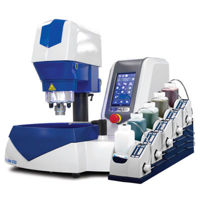
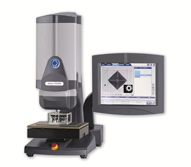
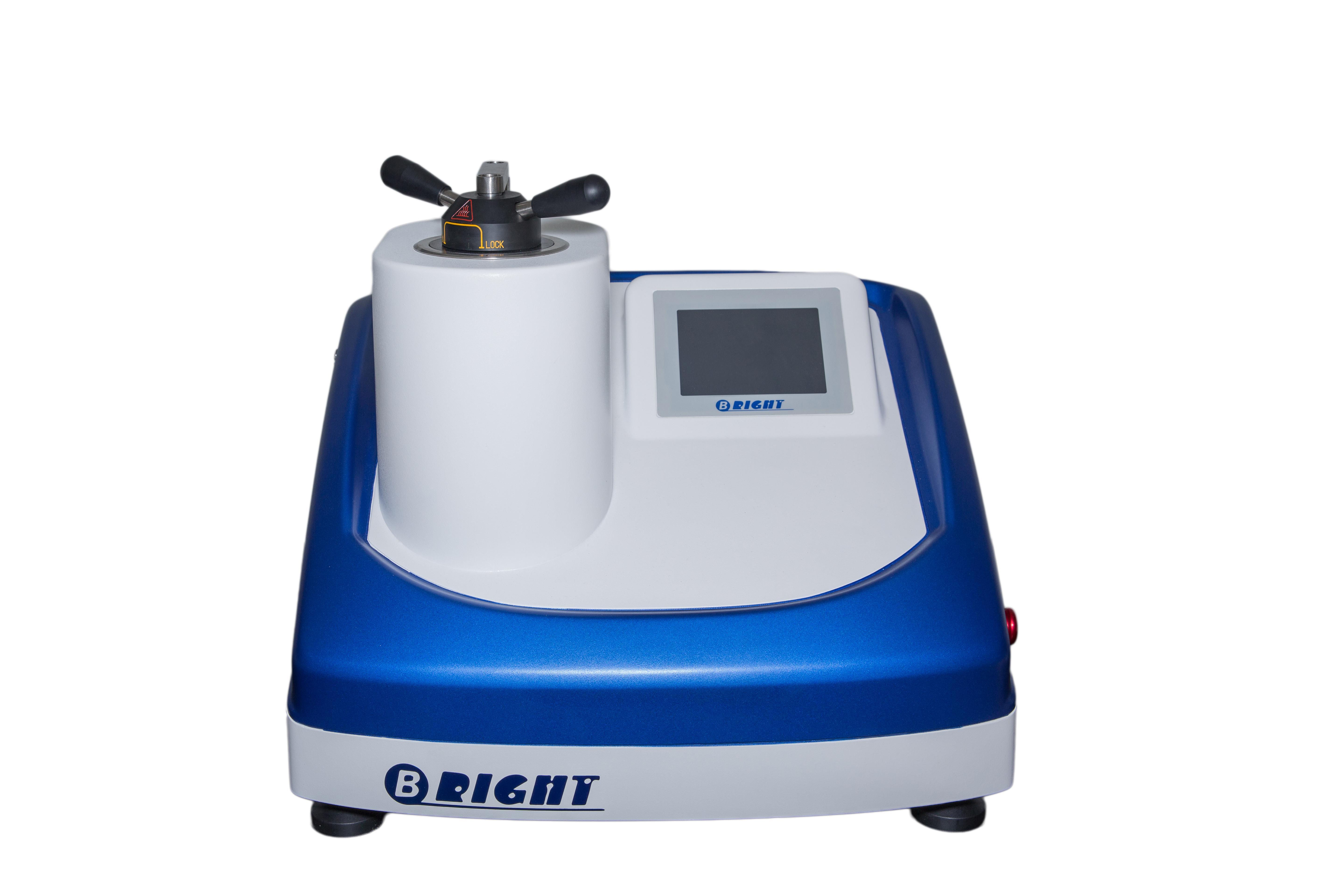
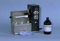
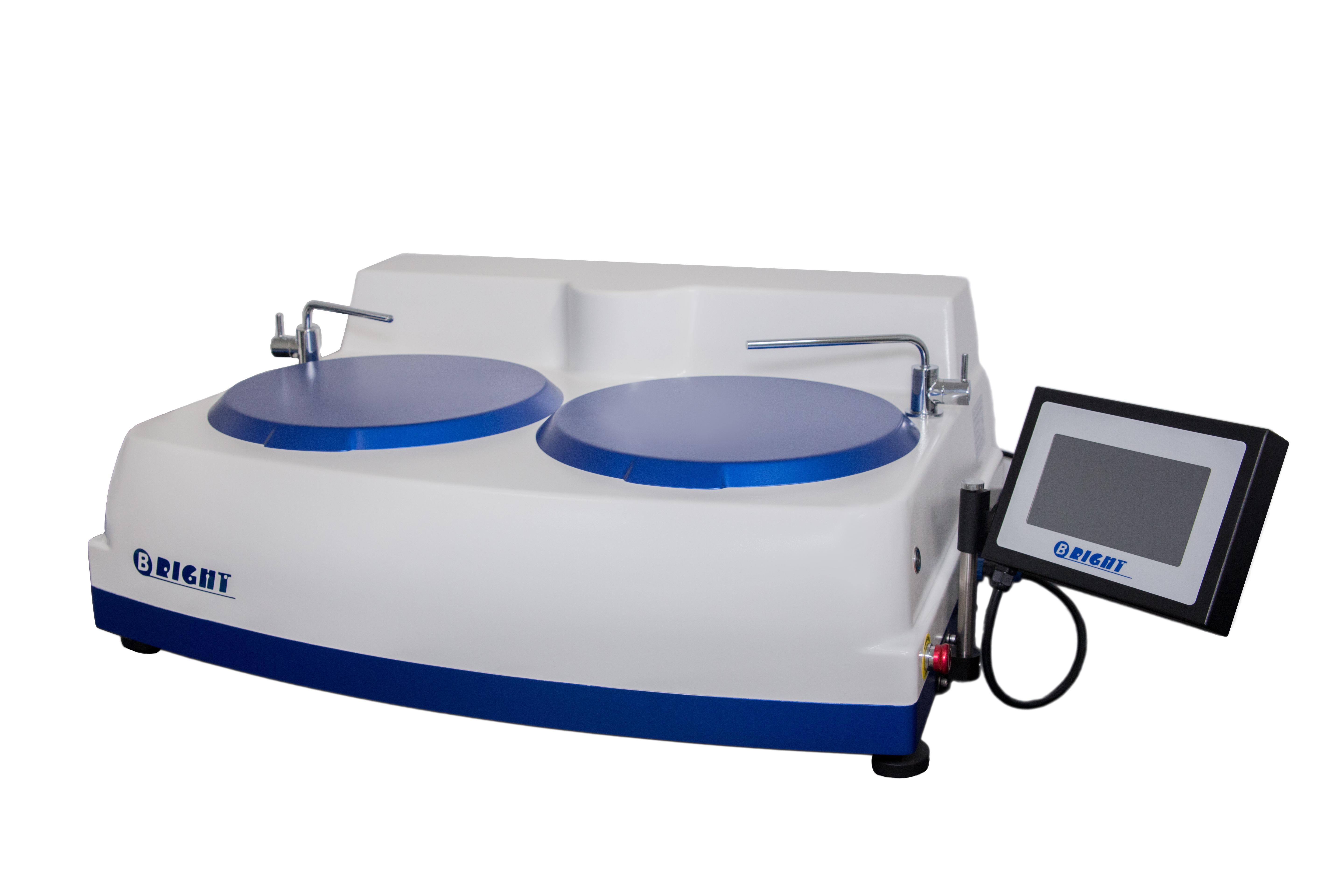
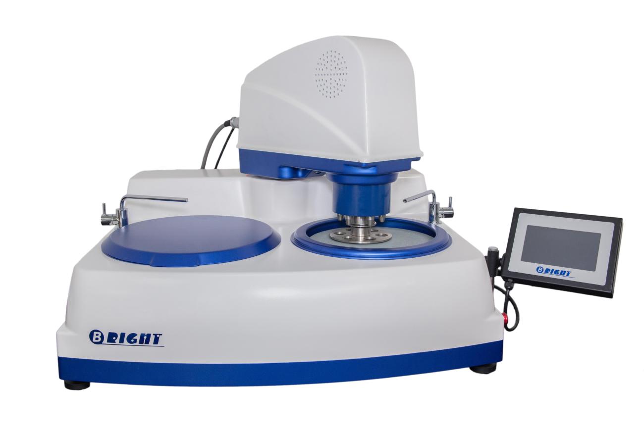
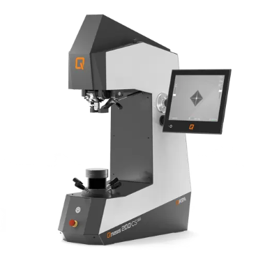
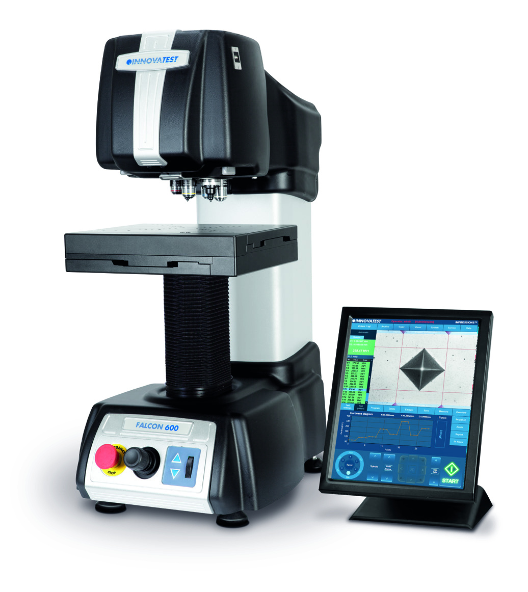
美国标乐为您提供《电子元器件中失效分析检测方案(镶嵌机)》,该方案主要用于电子元器件产品中失效分析检测,参考标准《暂无》,《电子元器件中失效分析检测方案(镶嵌机)》用到的仪器有Cast N' Vac 1000 真空镶嵌机、IsoMet™ 低速精密切割机、美国标乐 Buehler | AutoMet™ 250 研磨抛光机、全自动维氏/努氏硬度计 VH3300 | 美国威尔逊硬度计。
我要纠错
推荐专场
相关方案
 咨询
咨询