

方案详情文
智能文字提取功能测试中
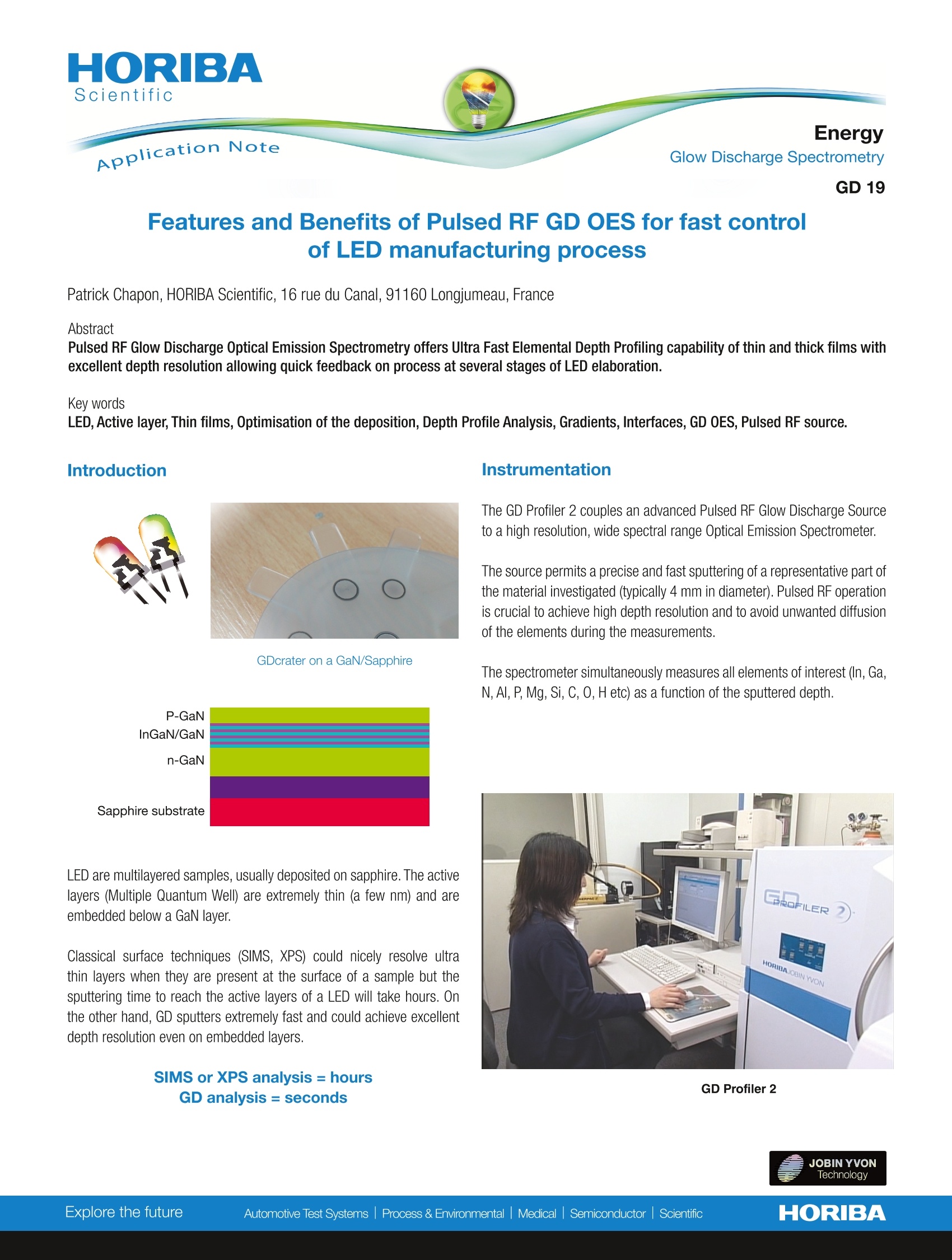
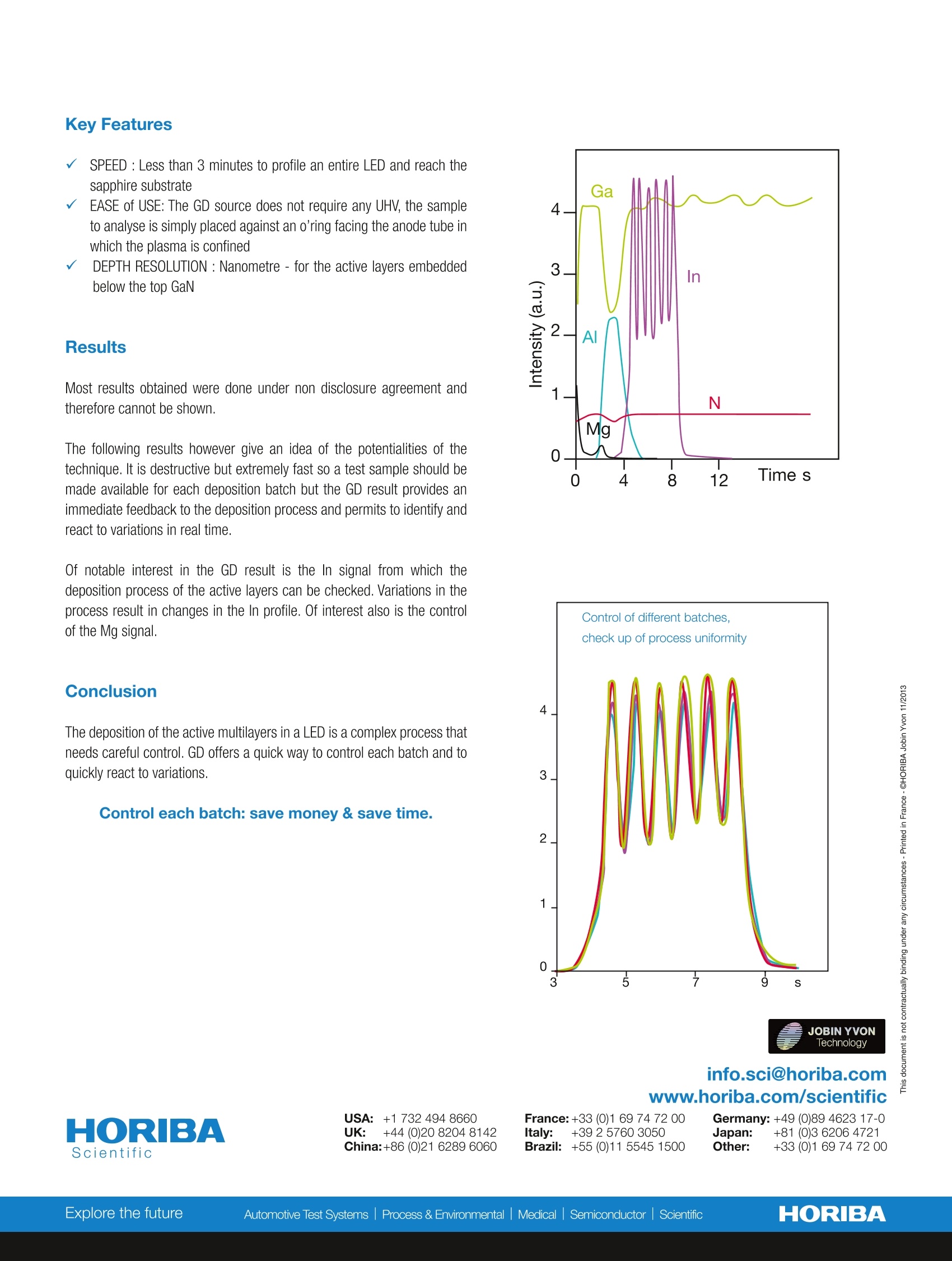
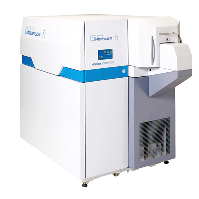
HORIBAScientific USA::+1732 494 8660UK: +44 (0)20 8204 8142China:+86 (0)21 6289 6060 Energy Application Note Glow Discharge Spectrometry GD 19 Features and Benefits of Pulsed RF GD OES for fast controlof LED manufacturing process Patrick Chapon, HORIBA Scientific, 16 rue du Canal, 91160 Longjumeau, France Abstract Pulsed RF Glow Discharge Optical Emission Spectrometry offers Ultra Fast Elemental Depth Profiling capability of thin and thick films withexcellent depth resolution allowing quick feedback on process at several stages of LED elaboration. Key words LED, Active layer, Thin films, Optimisation of the deposition, Depth Profile Analysis, Gradients, Interfaces, GD OES,Pulsed RF source. Introduction Instrumentation The GD Profiler 2 couples an advanced Pulsed RF Glow Discharge Sourceto a high resolution, wide spectral range Optical Emission Spectrometer. The source permits a precise and fast sputtering of a representative part ofthe material investigated (typically 4 mm in diameter). Pulsed RF operationis crucial to achieve high depth resolution and to avoid unwanted diffusionof the elements during the measurements. The spectrometer simultaneously measures all elements of interest (In, Ga,N, Al, P,Mg, Si, C, 0,Hetc) as a function of the sputtered depth. LED are multilayered samples, usually deposited on sapphire. The activelayers (Multiple Quantum Well) are extremely thin (a few nm) and areembedded below a GaN layer. Classical surface techniques (SIMS, XPS) could nicely resolve ultrathin layers when they are present at the surface of a sample but thesputtering time to reach the active layers of a LED will take hours.Onthe other hand, GD sputters extremely fast and could achieve excellentdepth resolution even on embedded layers. SIMS or XPS analysis = hoursGD analysis = seconds GD Profiler 2 √SPEED : Less than 3 minutes to profile an entire LED and reach thesapphire substrate EASE of USE: The GD source does not require any UHV, the sampleto analyse is simply placed against an o’ring facing the anode tube inwhich the plasma is confined DEPTH RESOLUTION : Nanometre- for the active layers embeddedbelow the top GaN Results Most results obtained were done under non disclosure agreement andtherefore cannot be shown. The following results however give an idea of the potentialities of thetechnique. It is destructive but extremely fast so a test sample should bemade available for each deposition batch but the GD result provides animmediate feedback to the deposition process and permits to identify andreact to variations in real time. Of notable interest in the GD result is the In signal from which thedeposition process of the active layers can be checked. Variations in theprocess result in changes in the In profile. Of interest also is the controlof the Mg signal. Conclusion The deposition of the active multilayers in a LED is a complex process thatneeds careful control. GD offers a quick way to control each batch and toquickly react to variations. Control each batch: save money & save time. JOBIN YVON Technology info.sci@horiba.comwww.horiba.com/scientific France:+33 (0)1 69 74 72 00 Germany:+49 (0)89 4623 17-0Italy: +39 2 5760 3050 Japan: +81 (0)3 6206 4721Brazil: +55 (0)11 5545 1500 Other: +33 (0)1 69 74 7200 Explore the futureHORIBAAutomotive Test Systems| Process & Environmentalalll MedicallSemiconductorScientific
关闭-
1/2
-
2/2
产品配置单
HORIBA(中国)为您提供《快速、深度剖析LED芯片的镀层结构》,该方案主要用于其他中null检测,参考标准《暂无》,《快速、深度剖析LED芯片的镀层结构》用到的仪器有HORIBA GD Profiler 2射频辉光放电光谱仪。
我要纠错
推荐专场

相关方案
 咨询
咨询