
方案详情文
智能文字提取功能测试中
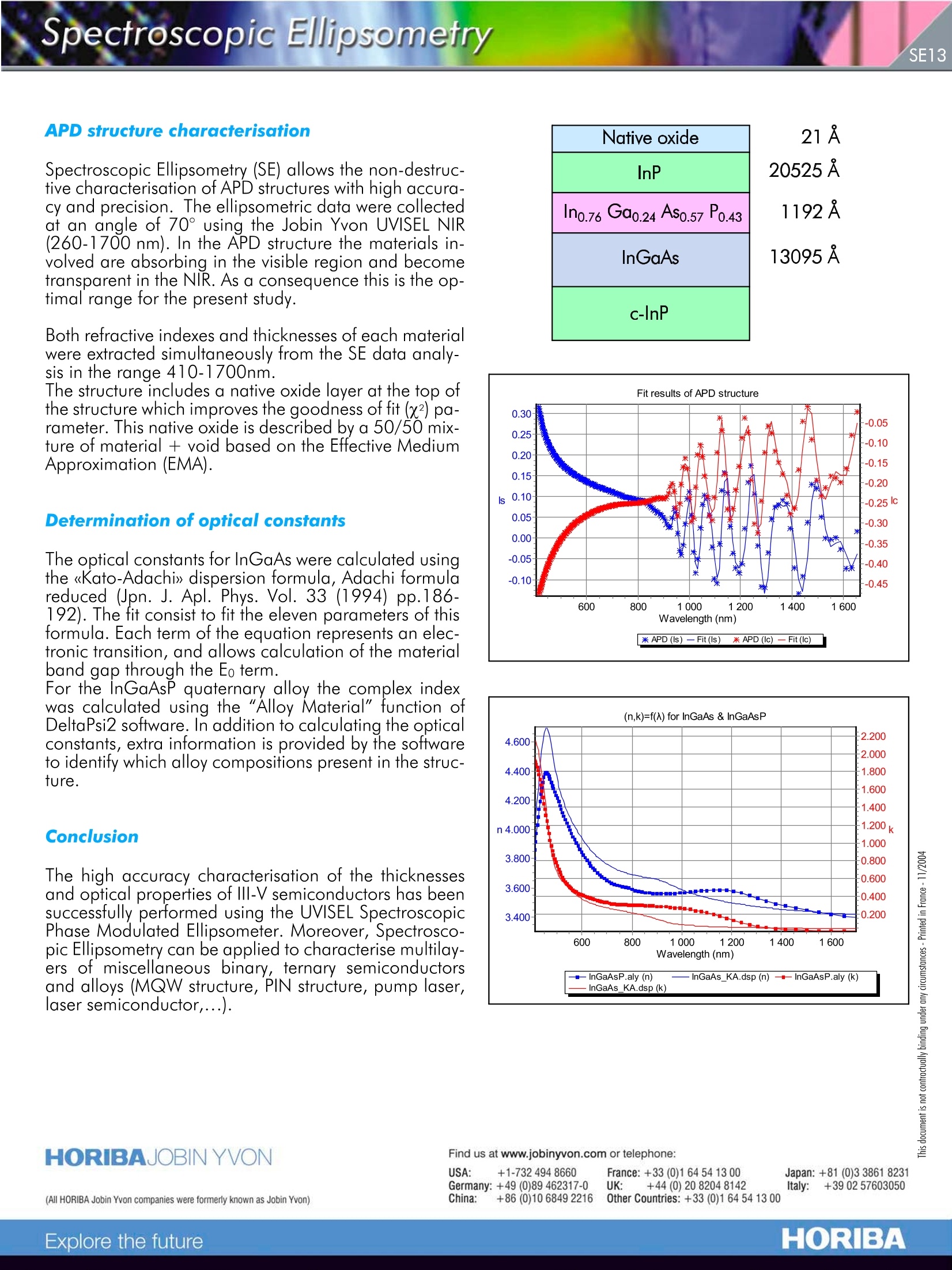
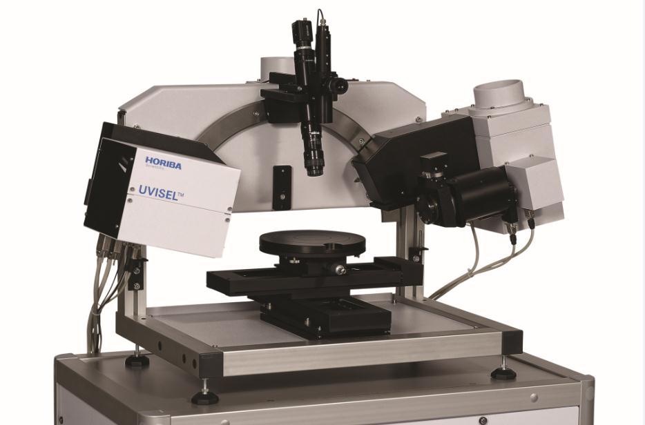
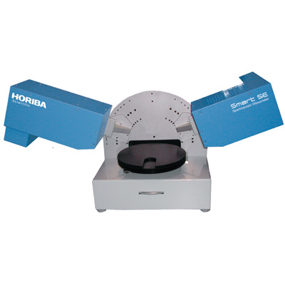
Application NoteSemiconductorUVISELSpectroscopic EllipsometrySE13 Spectroscopic Ellipsometry Celine Eypert -Application Scientist - Thin Film Division m-V semiconductors materials allow the manufacture of high performance optoelectronics andhypertrequency devices. One such device is the Avalanche Photodiodes (APD),and this is a promising solution to the increasing de-mand for high-performance optical transmission sys-tems to detect low optical signals in applications such asong-distance tibre communications, spectrometry andaser radars. However, several problems remain to beresolved tor their use as high-speed optical detectors.lhe problems include low reliability and narrow struc-tural margins tor very high-speed responses. Many researches have focused on improving their per-tormance via techniques such as band gap engineeringand optimization of device structures in -V compoundsemiconductors. These structures have offeredlargegain-bandwidth products and high performances at 1.3and 1.55 um wavelengths. To reach the desiredper-tormance multilayer alloy structures must be grown withaccurate thickness and composition using epitaxial re-actors such as MBE, MOVPE or MOCVD, and accu-rately characterisedusing nnon-destructivetestmethod. The UVISEL NIR Spectroscopic Ellipsometer provides afast, non destructive characterisation tool which hashelped to improve the manufacturing yield of APDs, Theaccuracy and reliability of the ellipsometric measure-ment has allowed replacement of the selective chemicaletch used to measure the thicknesses. The UVISEL Spec-troscopic Ellipsometer may also be applied to the char-acterisation of laser structures, photodetectors andmany other complex multilayer devices. How does an APD work? An avalanche photodiode is essentially a PIN or PNphotodiode operating at high reverse bias. At such a InGaAs APD Photodetector Epitaxial Structure high bias the free carriers (electrons and holes) in thedepletion region are accelerated to high speeds. Sucha carrier with high kinetic energy can excite an electronin the valence band to the conduction band and there-fore create an electron and a hole. This one-carrierthree-carrier process is called an impact ionization oravalanche process. As a result, the current is amplified. APD structure characterisation Spectroscopic Ellipsometry (SE) allows the non-destruc-tive characterisation of APD structures with high accura-cy and precision. The ellipsometric data were collectedat an angle of 70° using the Jobin Yvon UVISEL NIR(260-1700 nm). In the APD structure the materials in-volved are absorbing in the visible region and becometransparent in the NIR. As a consequence this is the op-timal range for the present study. Both refractive indexes and thicknesses of each materialwere extracted simultaneously from the SE data analy-sis in the range 410-1700nm. The structure includes a native oxide layer at the top ofthe structure which improves the goodness of fit (x?) pa-rameter. This native oxide is described by a 50/50 mix-ture of material + void based on the Effective MediumApproximation (EMA). Determination of optical constants The optical constants for InGaAs were calculated usingthe《Kato-Adachi》 dispersion formula, Adachi formular1e92d)u.c eTdhe Ufpint. c oJn.s iAstp lt.o Pfihty st.h eV eolle.v3e3n p(a1994) pp.186-rameters of thisformula Fash tarm of the eauation ranresants stronic transition, and allows calculation ot the materialhand aan through the Fa term, For the InGaAsP quaternary alloy the complex indexwas calculated using the "Alloy Material" function ofDeltaPsi2 software. In addition to calculating the opticalconstants, extra information is provided by the softwareto identify which alloy compositions present in the struc-ture. Conclusion The high accuracy characterisation of the thicknessesand optical properties of ⅢII-V semiconductors has beensuccessfully performed using the UVISEL SpectroscopicPhase Modulated Ellipsometer. Moreover, Spectrosco-pic Ellipsometry can be applied to characterise multilay-ers of miscellaneous binary, ternary semiconductorsand alloys (MQW structure, PIN structure, pump laser,laser semiconductor,...). 21A 20525A 1192 A 13095A HORIBAJOBIN YVONHORIBAExplore the future Find us at www.jobinyvon.com or telephone:(All HORIBA Jobin Yvon companies were formerly known as Jobin Yvon)HORIBAExplore the future The high accuracy characterisation of the thicknesses and optical properties of III-V semiconductors has been successfully performed using the UVISEL Spectroscopic Phase Modulated Ellipsometer. Moreover, Spectroscopic Ellipsometry can be applied to characterise multilayers of miscellaneous binary, ternary semiconductors and alloys (MQW structure, PIN structure, pump laser, laser semiconductor,…).
关闭-
1/2

-
2/2
产品配置单
HORIBA(中国)为您提供《III-V族半导体中厚度,光学常数检测方案(椭偏仪)》,该方案主要用于其他中厚度,光学常数检测,参考标准《暂无》,《III-V族半导体中厚度,光学常数检测方案(椭偏仪)》用到的仪器有HORIBA UVISEL Plus研究级经典型椭偏仪 。
我要纠错
相关方案
 咨询
咨询