方案详情文
智能文字提取功能测试中
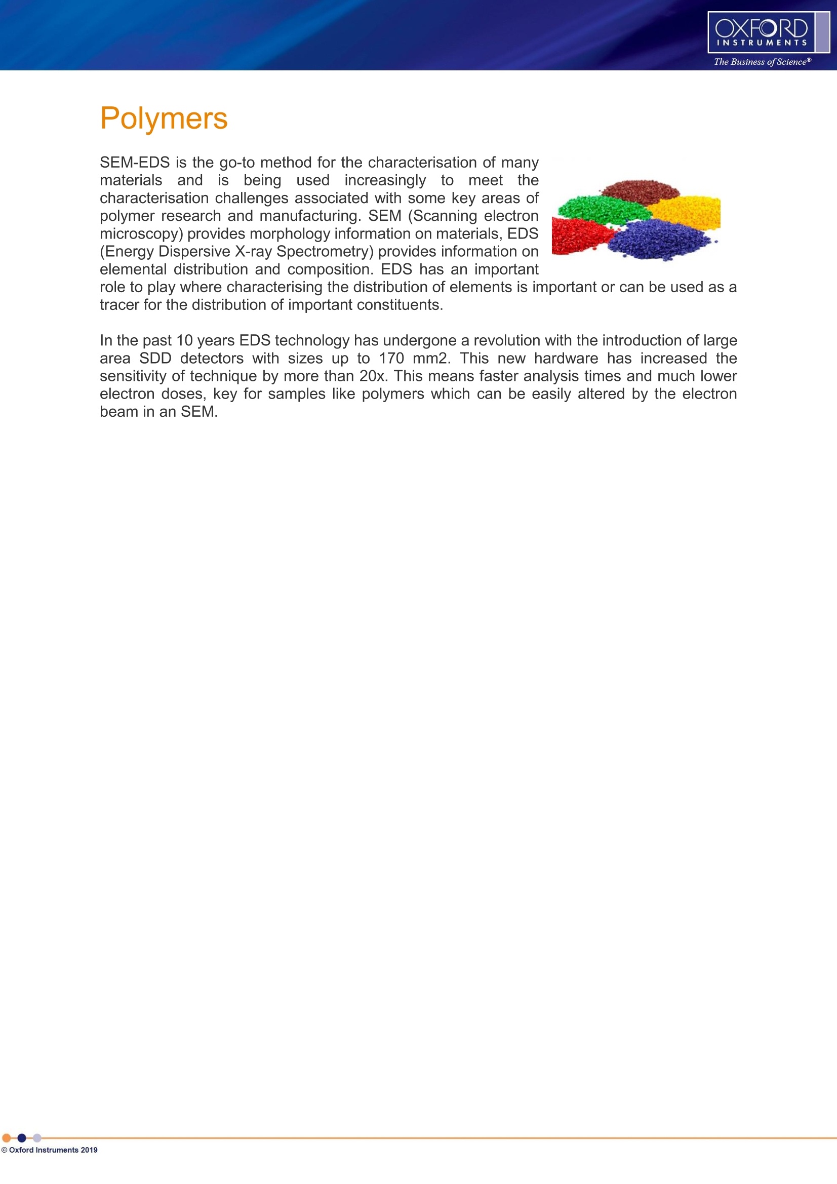
OXFORDINSTRUMEN T SThe Business ofScience@oxford Instruments 2019 Polymers SEM-EDS is the go-to method for the characterisation of manymaterialsandisbeingused increasinglyto)meettthecharacterisation challenges associated with some key areas ofpolymer research and manufacturing. SEM (Scanning electronmicroscopy) provides morphology information on materials, EDS(Energy Dispersive X-ray Spectrometry) provides information onelemental distribution and composition. EDS has an importantrole to play where characterising the distribution of elements is important or can be used as a tracer for the distribution of important constituents. In the past 10 years EDS technology has undergone a revolution with the introduction of largearea SDD detectors with sizes up to 170 mm2. This new hardware has increased thesensitivity of technique by more than 20x. This means faster analysis times and much lowerelectron doses, key for samples like polymers which can be easily altered by the electronbeam in an SEM. SEM-EDS is the go-to method for the characterisation of many materials and is being used increasingly to meet the characterisation challenges associated with some key areas of polymer research and manufacturing. SEM (Scanning electron microscopy) provides morphology information on materials, EDS (Energy Dispersive X-ray Spectrometry) provides information on elemental distribution and composition. EDS has an important role to play where characterising the distribution of elements is important or can be used as a tracer for the distribution of important constituents.In the past 10 years EDS technology has undergone a revolution with the introduction of large area SDD detectors with sizes up to 170 mm2. This new hardware has increased the sensitivity of technique by more than 20x. This means faster analysis times and much lower electron doses, key for samples like polymers which can be easily altered by the electron beam in an SEM.
关闭-
1/1
产品配置单

牛津仪器科技(上海)有限公司为您提供《高聚物中镀膜检测方案 》,该方案主要用于高聚物中镀膜检测,参考标准《暂无》,《高聚物中镀膜检测方案 》用到的仪器有牛津仪器Azteclive能谱实时元素成像系统。
我要纠错
相关方案
 咨询
咨询