


 仪器对比
仪器对比


 关注
关注
 样本下载
样本下载
Company Profile
SemiMap Scientific Instruments GmbH develops measurement systems to evaluate electrical properties of semi-insulating compound semiconductor substrates. GaAs, InP, SiC, GaN and CdTe wafers are chearacterized by SemiMap systems with respect to resistivity, mobility and carrier concentration.
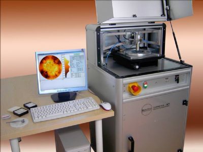
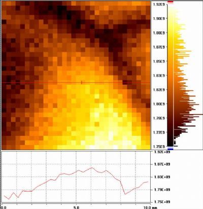
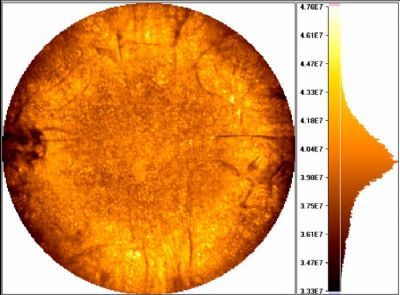
The non-destrucive contactless capacitive measurement technique requires no sample preparation and generates full wafer resistivity topograms revealing lateral variations as small as 1% with high lateral resolution.
SemiMap Analytical Systems
Evaluation of electrical material properties
Resistivity r = Q0 t (Q¥ e e0) -1
Mobility µ = 1/B [ r(B) / r(0) - 1] ½
Activation energy Ea = (kT1T2)/(T2-T1) * ln [r(T1) / r(T2)]
COREMA-WT | Measures susbtrate resistivity. Contactless mapping of wafers up to 200 mm in diameter, 1 mm resolution; resistivity range 1x10⁵ to 1x10¹² W-cm; automated measurement routines, statistical analysis. |
COREMA-VT
| Measures substrate resistivity at variable temperature range from room temperature up to 400 oC; evaluation of carrier activation energy via Arrhenius plot |
COREMA-ER
| Measures sheet resistance (>105 W) of epitaxial buffer layers; calculate layer resistivity for given thickness. |
======================================================================================================
 | COREMA - WT 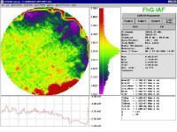  |
The COntactless REsistivity MApper designed for Wafer Topography (COREMA - WT) is a high performance diagnostic tool to characterize the resistivity of semi-insulating semiconductor wafers with utmost precision, repeatability and detail. Full wafer resistivity topograms discern fluctuations in the percent range with lateral resolution below 1 mm. It is used for routine production control as well as in-depth analysis supporting material development. Analytic methods to discern and quantify locally inhomogeneous material have been elaborated.
=====================================================================================================
| COREMA - RM |
The COREMA - RM system determines the full set of electrical transport parameters (Resistivity, carrier Mobility and carrier concentration). It replaces completely the conventional Hall measurements by a contactless procedure which is vastly superior in speed and reproducibility. Data may be taken at any desired spot on wafers up to 200 mm.
• Probe diameter 1 mm
• Sample diameter 10 mm – 100 mm
• Manual loading
• Free choice of measurement position
• Mobility > 1000 cm2/Vs
ISSUE | CONVENTIONAL HALL | COREMA - RM |
Wafer cutting | necessary | Non-destructive |
Ohmic contacts | needed, critical | obsolete |
Sample preparation | ~ 15 min | none |
Sample insertion and measurement time | ~ 10 min | ~ 30 s |
Repeatability | ~ 5% | < 1% |
Evaluation of SI material | difficult | easy |
Applicability | general |
SI material only |
Acceptance | standard method | new method |
=======================================================================================================
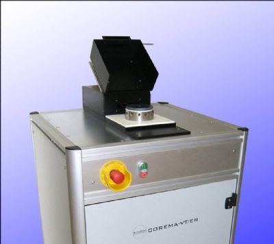
| COREMA -VT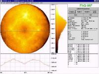 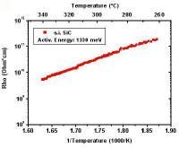 |
The COREMA - VT system is designed to measure resistivity at Variable Temperature above RT up to 600 K. It is primarily used to characterize SiC wafer material for verification of high temperature specifications and for detailed analytic support of material development. Data may be taken at any desired spot on wafers up to 200 mm.
System designed to evaluate resistivity at Variable Temperature
• Temperature range 300 K – 673 K (RT – 400 C)
• Resistivity range 1 x 10 5 – 1 x 10 12 Ωcm
• High temperature capacitive probe design
• Probe diameter 8 mm
• Sample diameter 10 mm – 100 mm
• Manual loading
• Free choice of measurement position
======================================================================================================
| COREMA -ER  |
The COREMA - ER system is designed to measure thin epitaxial layers with intermediate resistivity, grown on high resistivity substrates (Epitaxial layer, Resistivity). The most important application presently appears to be the control and analysis of GaN buffer layers on s.i. SiC or Sapphire. The procedure is not applicable to evaluate conducting layers, as used in active devices (e.g. HEMTs). Presently layers with a resistance from 1E5 Ohm to 1E11 Ohm can be measured. Consequently, for a typical layer thickness of 1 µm, the measured resistivity range is 10 Ohm*cm to 1E7 Ohm*cm. The range shifts to lower (higher) resistivity for thinner (thicker) layers. As a side condition, the substrate resistance must be large compared to the layer resistance. For a 1 µm layer this means that the substrate resistivity must exceed the layer resistivity by at least a factor of 1E4. This condition can be relaxed if the substrate resistance is known and taken into account in the analysis.
The procedure is designed to measure thin epitaxial layers with intermediate resistivity, grown on high resistivity substrates.
The most important application presently appears to be the control and analysis of GaN buffer layers on SiC or Sapphire.
The procedure is not applicable to evaluate conducting layers, as used in active devices (e.g. HEMTs).
====================================================================================================
Contacts
Saratoga Technology International
美国赛伦科技为SemiMap中国总经销
赛伦科技上海办事处
上海市黄浦区陆家浜路1378号万事利大厦
吴惟雨/ Caven Wu
| 用户单位 | 采购时间 |
|---|---|
| Shandong University | 2012-06-19 |
| Tianjin Electronic Material Research Institute | 2012-01-08 |
| CETC No.2 Reserch Institute | 2011-03-08 |
| Beijing HJCW | 2010-01-10 |
根据合约
是
无
根据合约
根据合约
根据合约
根据合约


相关产品

