

 仪器对比
仪器对比


 关注
关注
 样本下载
样本下载
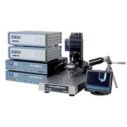
Sciospec ISX-3v2 – Electrical Impedance Spectroscopy
Measurement Parameters
![]()
impedance | absolute value of impedance, phase of impedance in degree, phase of |
impedance in radiant, resistance, reactance, absolute value of | |
admittance, phase of admittance in degree, phase of admittance in | |
radiant, conductance, susceptance | |
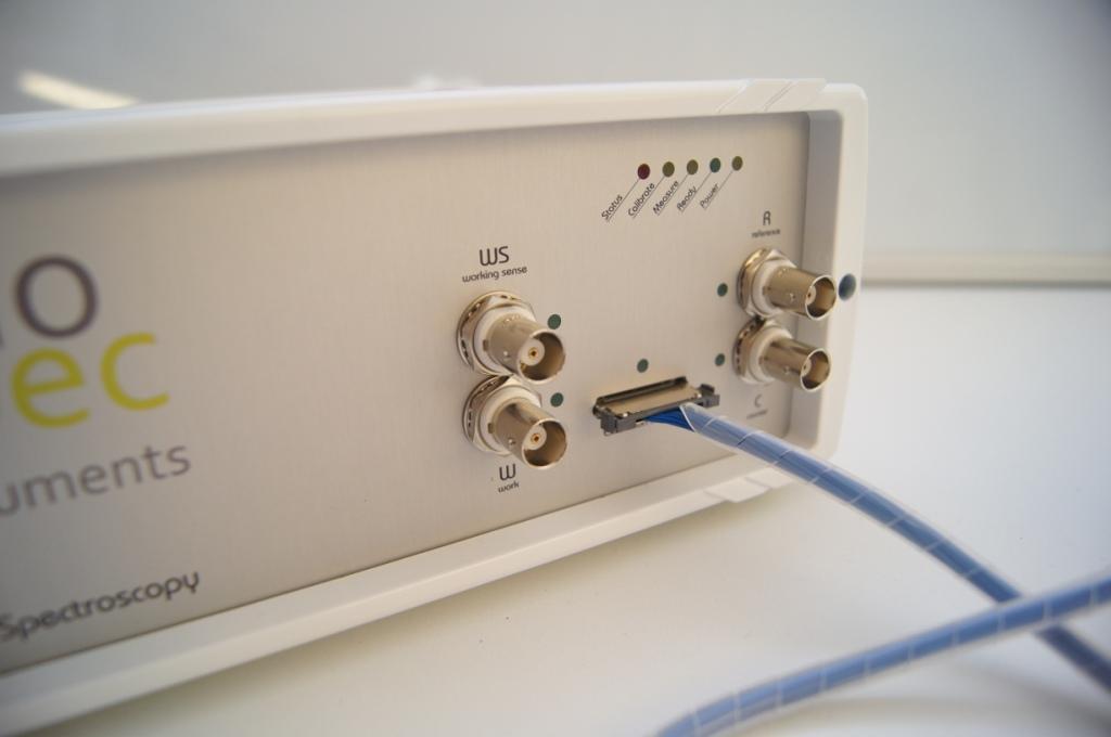
Measurement Terminal | |
configuration | four wire configuration, three wire configuration, two wire |
configuration (counter C, reference R, work W, working Sense WS) | |
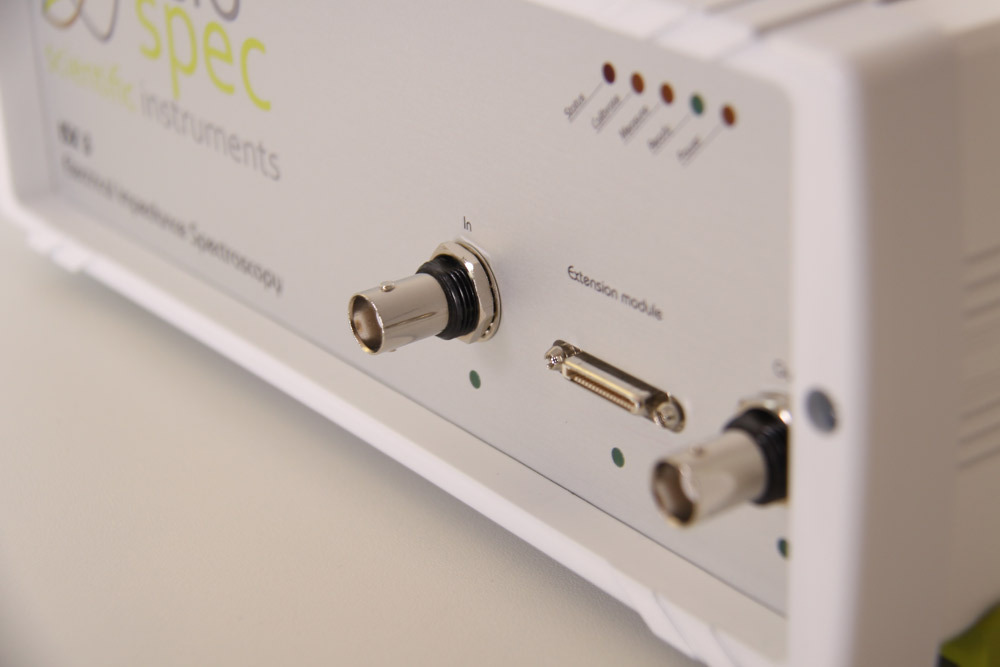
connector type | four BNC (female, standard polarity) connectors, |
Sciospec ExtensionPort | |
Sciospec ExtensionPort | |
connector type | Samtec FCS8 20 Pin |
signal level standard | LVCMOS 3V |
maximum input voltagei | 3.6V |
minimum input voltage | -0.3V |
high level input voltage | ≥1.7V |
low level input voltage | 0.8V |
high level output voltage | ≥2.8V |
maximum output current | 12mA |
ESD protection of IOs | ±12kV IEC 61000-4-2 contact ESD |
±15kV IEC 61000-4-2 air-gap ESD | |
clamp voltage 10.5V (min) | |
break-down voltage 7V (min) | |
number of IOs | eight total (freely distributable between input and output) |
IO configuration | GPIO, UART, I2C |
measurement terminals | four (counter C, reference R, work W, working sense WS) |
power terminals | ±5V; 500mA for each voltage |
pin assignment | see Tab 1, shielding GND |
connector Layout | see Fig 1 |
![]()
![]()
![]()
Data she e t Sci o spe c I SX - 3v 2
J une 20 14
![]()
PIN | ||||||||||||||||||||
1 | 2 | 3 | 4 | 5 | 6 | 7 | 8 | 9 | 10 | 11 | 12 | 13 | 14 | 15 | 16 | 17 | 18 | 19 | 20 | |
Mode | ||||||||||||||||||||
GPIO | W | +5V | +5V | +5V | +5V | WS | IO1 | IO2 | IO3 | IO4 | IO5 | IO6 | IO7 | IO8 | R | -5V | -5V | -5V | -5V | C |
I2C | W | +5V | +5V | +5V | +5V | WS | SCK1 SDA1 | SCK2 | SDA2 | d.n.c. | d.n.c. | d.n.c. | d.n.c. | R | -5V | -5V | -5V | -5V | C | |
UART | W | +5V | +5V | +5V | +5V | WS | Rx | Tx | d.n.c. | d.n.c. | d.n.c. | d.n.c. | d.n.c. | d.n.c. | R | -5V | -5V | -5V | -5V | C |
Tab 1: ExtensionPort pin assignment for differnet modes of operation
![]()
Fig 1: ExtensionPort Pin Assignment
Frequency
range | 100mHz to 10MHz | |
resolution | 10mHz (depending on frequency range setting) | |
precision absolute | ±100ppm (at 25°C) | |
temperature drift | ±10ppm over operating temperature range | |
long time stability | ±5ppm first year | |
Voltage Signal | ||
range | 1mV to 1000mV peak-amplitude | |
resolution | 0.1 mV | |
Output Impedance | ||
output impedance | 300? (nominal) | |
DC Bias | ||
voltage range | 0V to 8V (see Fig 7) | |
voltage resolution | 10 mV | |
current range | 0A to 20mA (see Fig 7) | |
current resolution | 25μA | |
Precision settings | ||
precision range | 0 to 1 high speed, lower accuracy | |
1 | standard configuration |Z|/|Z|<0.1% | |
1 to 10 high accuracy, low speed | ||
averaging | 1 to 1024 | |
![]()
![]()
![]()
![]()
![]()
![]()
![]()
Data she e t Sci o spe c I SX - 3v 2
J une 20 14
Sweep Settings
![]()
available sweep | frequency, amplitude, DC bias voltage, DC bias current, kinetic, |
parameters | point delay |
sweep type | linear, logarithmic, list |
points | 1 to 2048 |
sweep delayii | 0s to 3min in 1μs steps |
point delayiii | 0s to 3min in 1μs steps |
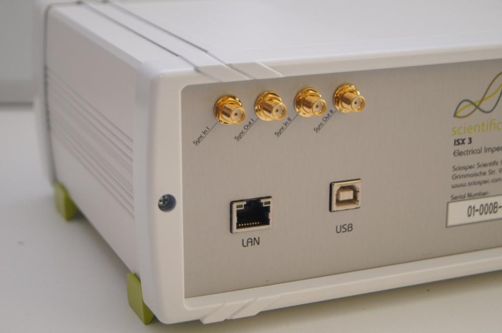
Synchronisation Ports (SyncPort) | |
sync ports | two inputs, two outputs, |
sync input type | point hold off, sweep hold off, immediate stop |
sync output type | sweep complete, point complete |
connectors | four SMA (female, standard polarity) |
ESD protection | ±12kV IEC 61000-4-2 contact ESD |
±15kV IEC 61000-4-2 air-gap ESD | |
clamp voltage 10.5V (min) | |
break-down voltage 7V (min) | |
absolute maximum input | 5.5V |
absolute minimum input | -0.3V |
voltage | |
high level input voltage | ≥2V |
low level input voltage | ≤0.8V |
high level output voltage | ≥2.7V (open drain buffer with 1kOhm pull up resistor to 3V) |
low level output voltage | ≤0.55V |
maximum output current | 24mA |
typical input capacitance | 3pF |
IO Port (optional) | |
connector type | D-Sub-Mikro-D 20Pin |
signal level standard | LVCMOS 3V |
absolute maximum input | 3.6V |
absolute minimum input | -0.3V |
voltage | |
high level input voltage | ≥1.7V |
low level input voltage | ≤0.8V |
high level output voltage | ≥2.8V |
low level output voltage | ≤0.2V |
maximum output current | 12mA |
ESD Protection of IOs | ±12kV IEC 61000-4-2 contact ESD |
±15kV IEC 61000-4-2 air-gap ESD | |
clamp voltage 10.5V (min) | |
break-down voltage 7V (min) | |
number of IOs | eight (freely distributable between input and output) |
![]()
![]()
![]()
Data she e t Sci o spe c I SX - 3v 2
J une 20 14
IO configuration | GPIO, UART, I2C | ||||||||||||||||||||||||
UART configuration | 115.2kBaud, 1 start bit, 8 data bits, 1 stop bit, even polarity, idle high | ||||||||||||||||||||||||
I2C configuration | 100kbit, 7bit address, standard mode, device behaves as master | ||||||||||||||||||||||||
number of | 2 | ||||||||||||||||||||||||
temperature sensors | |||||||||||||||||||||||||
temperature sensor type | Negative temperature coefficient (NTC) | ||||||||||||||||||||||||
configurable: Reference resistance, reference temperature, Beta value | |||||||||||||||||||||||||
pin assignment | See Tab 2 | ||||||||||||||||||||||||
connector layout | See Fig 2 | ||||||||||||||||||||||||
PIN | 1 | 2 | 3 | 4 | 5 | 6 | 7 | 8 | 9 | 10 | 11 | 12 | 13 | 14 | 15 | 16 | 17 | 18 | 19 | 20 | |||||
Mode | |||||||||||||||||||||||||
GPIO | GND | NTC1 | GND | NTC2 | GND | IO1 | GND | IO2 | GND | IO3 | GND | IO4 | GND | IO5 | GND | IO6 | GND | IO7 | GND | IO8 | |||||
I2C | GND | NTC1 | GND | NTC2 | GND | SCK1 | GND | SDA1 | GND | SCK2 | GND | SDA2 | GND | d.n.c. | GND | d.n.c. | GND | d.n.c. | GND | d.n.c. | |||||
UART | GND | NTC1 | GND | NTC2 | GND | Rx | GND | Tx | GND | d.n.c. | GND | d.n.c. | GND | d.n.c. | GND | d.n.c. | GND | d.n.c. | GND | d.n.c. | |||||
![]() Tab 2: IO Port pin assignment for different modes of operation
Tab 2: IO Port pin assignment for different modes of operation

Fig 2: IO Port connector
LAN Interface
standard conformity | 10/100 Base-T, RJ45 |
protocol | TCP/IP |
USB Interface | |
standard conformity | USB 2.0 Type B |
protocol | High Speed USB |
General Specifications | |
power requirements | 100-240V AC (typ.), 50/60Hz, 15W (max) |
dimensions | 248.67mm x 97.1mmx 193.2mm (width x height x depth) |
weight | 2.5kg (typical) |
operating conditions | 0°C to 40°C, <80% relative humidity non condensing, 0...3000m altitude |
non-operating conditions | -25°C to 80°C, <80% relative humidity non condensing1 |
![]()
![]()
![]()
Data she e t Sci o spe c I SX - 3v 2
J une 20 14

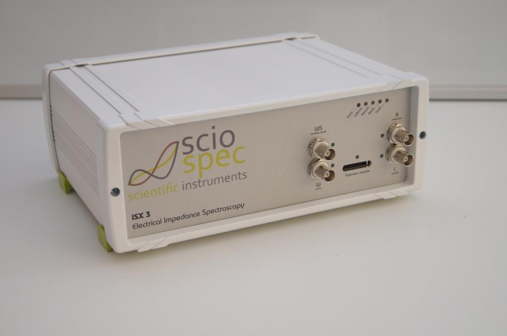
Fig 3: ISX-3v2 front view
![]()

Fig 4: ISX-3v2 side view
Specifications
All specifications above are stated for operation at temperatures between 0°C and 40°C. Warm-up time must be greater than or equal to 30 minutes after power on for all specifications.
Electro static discharge Warning
![]()
This product, like all electronic products, uses semiconductors that can be damaged by electrostatic discharge (ESD). When handling, care must be taken so that the devices are not damaged. Damage due to inappropriate handling is not covered by the warranty.
![]()
Data she e t Sci o spe c I SX - 3v 2
J une 20 14
Relation between the precision setting and the measurement time and measurement accuracy
The diagram on the left shows the influence of the precision settings on the accuracy and time for the measurement of an impedance value
![]()
at the specified frequency.
![]()
![]()
Low precision settings correspond to fast measurements with lower accuracy. High precision settings correspond to greater accuracy at longer measurement times.
![]()
![]()
![]()
Fig 5: Accuracy over Precision Parameter
![]()
10s | ||||||||
1s | ||||||||
100 ms | Prec | 10. | ||||||
Prec | 4. | |||||||
10ms | Prec | 2. | ||||||
Prec | 1. | |||||||
Prec | 0.5 | |||||||
Prec | 0. | |||||||
1ms | ||||||||
100 mHz | 1Hz | 10Hz | 100 Hz | 1kHz | 10kHz 100 kHz 1MHz | 10MHz | ||
Fig 6: Measurement Time over Precision Parameter
DC Bias Ranges
10V | |||||||
8V | |||||||
Voltage | 6V | ||||||
Bias | 4V | ||||||
2V | |||||||
0V | |||||||
0A | 5mA | 10mA | 15mA | 20mA | 25mA | ||
Bias | Current |
![]()
Fig 7: DC Bias Range
![]()
Data she e t Sci o spe c I SX - 3v 2
J une 20 14
Overview of the different range and precision settings

![]()
![]()
Data she e t Sci o spe c I SX - 3v 2
J une 20 14
![]()

Fig 8: Precision-Range Plot
All specifications refer to measurements done with a Sciospec ISX-3v2 in combination with the Sciospec MEArack. The signal amplitude is set to 100mV and the frequency range to ?<10MHz“. Measurements done, using the BNC connectors show very similar results.
![]()
Data she e t Sci o spe c I SX - 3v 2
J une 20 14
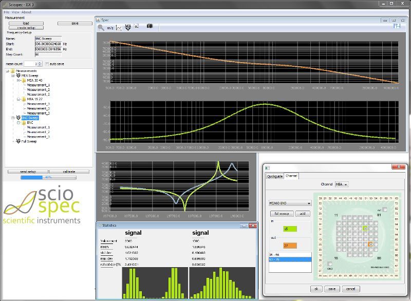
Example measurement:
Frequency sweep: 100Hz – 1MHz, 80 logarithmic Frequency steps, precision 1, amplitude 100mV, measurement range MΩ
Measurement instrument: Sciospec ISX-3v2 with connected Sciospec MEArack
DUT: Multielectrode array, 40μm electrodes, 200μm apart, platinum PBS buffersolution
![]()
![]()


- 相关仪器
相关产品

