方案详情文
智能文字提取功能测试中
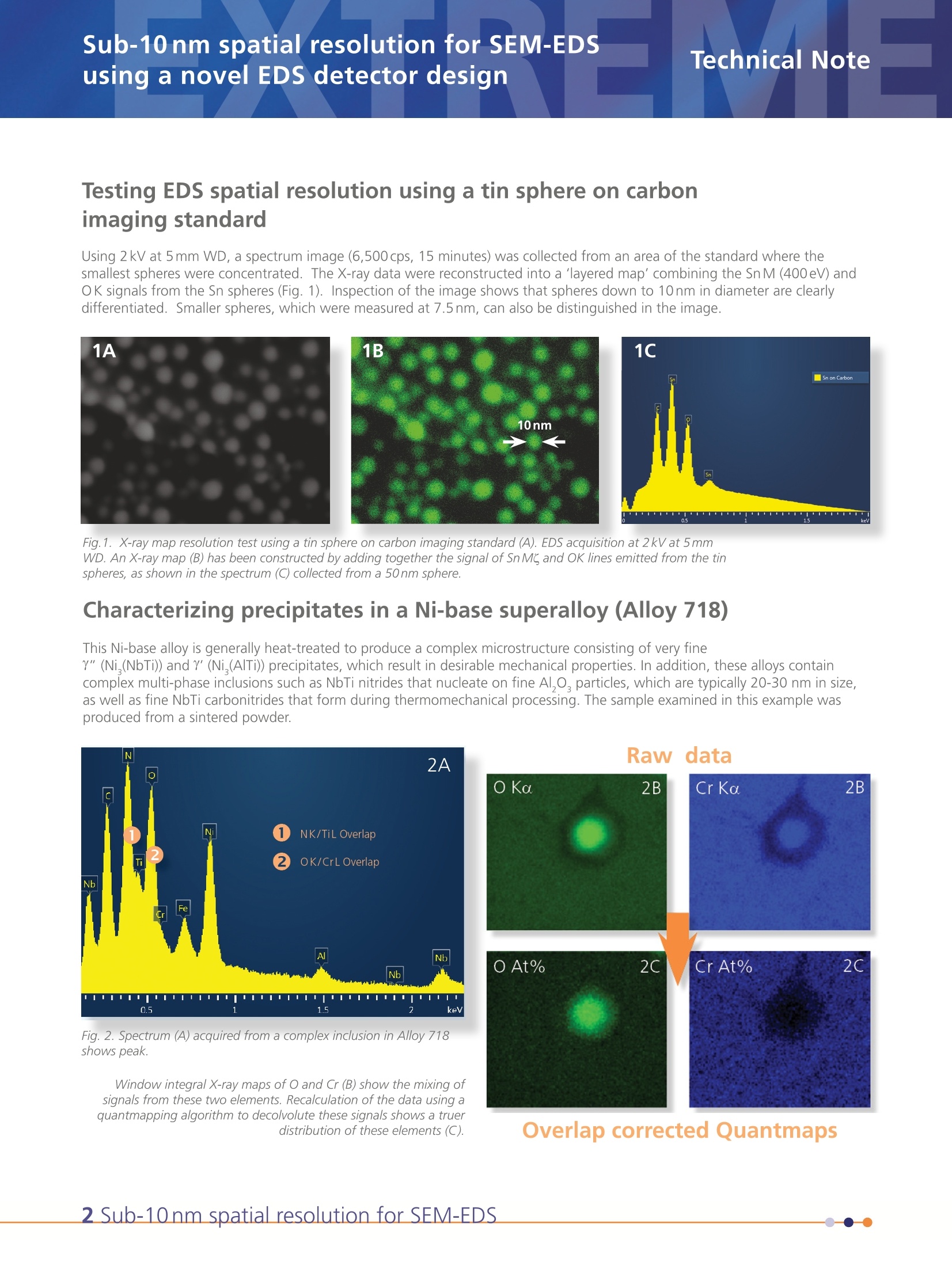
Technical Note Sub-10nm spatial resolution for SEM-EDSTechnical Noteusing a novel EDS detector design Sub-10nm spatial resolution for SEM-EDSusing a novel EDS detector design Introduction Limits to the practical spatial resolution and surface sensitivity of EDS analysis in the SEM are controlledby many factors, the dominant factor being microscope accelerating voltage. When the acceleratingvoltage is reduced to 1 kV, the volume from which X-rays are generated is reduced to around 10nmor less in many materials. However, the following side-effects may limit the potential for EDS analysis:loss of X-ray intensity, reduced choice of excited X-ray lines, increased microscope beam diameter, andincreased sensitivity to surface contamination. For this study a new windowlessdetector called X-Max Extremehas been designed using lownoise electronics and a highresolution 100 mm² SDDsensor. To maximize spatialresolution and sensitivity, theconventional detector geometryhas been radically altered. Tosignificantly increase count ratesunder very low kV microscopeconditions, the solid anglehas been increased by halvingthe distance between sampleand sensor and incorporatinga much smaller electron trap design. This geometry also allows the detector to collect X-rays when working at short working distance(5 mm or less) to minimize beam size and maximize surface-sensitive image contrast from in-lens electrondetectors. Using this new detector technology and current ultra-high resolution FEG-SEM capability (Zeiss Merlinand FEI Magellan/Helios), the practical limitations for high spatial resolution analysis in the SEM havebeen investigated. This has focused on the investigation of samples at 1.5-3kV to minimize the X-rayinteraction volume, necessitating the use of transition metal L lines, low energy K lines and, in particular,very low energy lines such as Nb Me for analysis. The Business ofScience@ Testing EDS spatial resolution using a tin sphere on carbonimaging standard Using 2 kV at 5 mm WD, a spectrum image (6,500 cps, 15 minutes) was collected from an area of the standard where thesmallest spheres were concentrated. The X-ray data were reconstructed into a 'layered map' combining the Sn M (400 eV) andOK signals from the Sn spheres (Fig. 1). Inspection of the image shows that spheres down to 10 nm in diameter are clearlydifferentiated. Smaller spheres, which were measured at 7.5 nm, can also be distinguished in the image. Fig.1. X-ray map resolution test using a tin sphere on carbon imaging standard (A). EDS acquisition at 2 kV at 5 mmWD. An X-ray map (B) has been constructed by adding together the signal of Sn MK and OK lines emitted from the tinspheres, as shown in the spectrum (C) collected from a 50nm sphere. Characterizing precipitates in a Ni-base superalloy (Alloy 718) This Ni-base alloy is generally heat-treated to produce a complex microstructure consisting of very fineY" (Ni (NbTi)) and Y'(Ni (AlTi)) precipitates, which result in desirable mechanical properties. In addition, these alloys containcomplex multi-phase inclusions such as NbTi nitrides that nucleate on fine Al,O, particles, which are typically 20-30 nm in size,as well as fine NbTi carbonitrides that form during thermomechanical processing. The sample examined in this example wasproduced from a sintered powder. Raw (data Fig.2. Spectrum (A) acquired from a complex inclusion in Alloy 718shows peak. Window integral X-ray maps of Oand Cr (B) show the mixing ofsignals from these two elements. Recalculation of the data using aquantmapping algorithm to decolvolute these signals shows a truerdistribution of these elements (C). Overlap corrected Quantmaps Characterization of complex nitride and oxide inclusions at 3kV A spectrum image was collected at 3kV and 3.5 mm working distance, at a count rate of 15,000 cps for 22 minutes. 3kVwas chosen to excite the NbL lines. X-ray maps reconstructed from this dataset showed clear errors due to overlaps of lowenergy peaks (e.g. NK/TiL and OK/CrL); therefore, the data were recalculated using a pixel-by-pixel 'QuantMap'algorithm todeconvolute peaks and remove background (Fig.2). The QuantMaps (Fig. 3) show that the elemental distribution in complexprecipitates of this scale can now be studied, and the N/Ti/Nb components can be successfully separated from the O/Alcomponents. To improve spatial resolution further requires the use of lower accelerating voltages. The soft X-ray lines available at very low kVcan undergo absorption, which presents a challenge to this technique. In Fig.4 the NbM line (170 eV) X-ray map has beenconstructed from the spectrum image dataset of the complex inclusion. This reveals only half of the NbTiN inclusion observedin other maps because Nb Mk X-rays furthest from the detector are absorbed strongly by the Al in the alumina inclusion.Collecting data from a further inclusion, at a lower accelerating voltage of 1.5 kV where this Mg line is required to characterizeNb distribution, shows this absorption phenomenon is clearly decreased due to the concentration of X-ray emission nearer the surface. Fig. 3. In lens electron image (A)and X-ray Quantmaps (B) froma complex inclusion in Alloy 718collected at 3kV and 3.5mmworking distance. Fig. 4. NbM map (A) from thecomplex inclusion collected at3kV shows a loss of signal in theregion furthest from the detector. Nb Mk X-ray map collected at1.5kV (4C) shows much lowerloss of signal in the regionfurthest from the detector. A spectrum (B) reconstructed from spectrum image datafrom this type of inclusion shows the available X-raylines available at a lower accelerating voltage of 1.5kVincluding Nb MC at 170eV. EDS characterization of microstructure of matrix at 1.5kV The microstructure of Alloy 718 consists of a high proportion of ordered Y" and Y' precipitates in a face-centred cubic matrix.These very fine precipitates exhibit well-known morphologies: the DO,,-ordered Y" precipitates are disc-shaped, and form withthe (001) (disc face) parallel to the matrix {100} planes, whereas the L1,-ordered Y' precipitates are cuboidal and exhibit a cube-cube orientation relationship with the matrix. The Y" and Y' precipitates are generally characterized using analytical transmissionelectron microscopy. Scanning electron microscopy can be effective for studying precipitate morphology, but it is important tonote that some of these precipitates have dimensions less than 10nm, making conventional 5-20 kV EDS analyses impractical. EDS spectrum imaging at different accelerating voltages (3, 2 and 1.5kV) showed the need for as low an accelerating voltageas possible in order to assess the chemical variations in this microstructure. A spectrum image was collected at 1.5 kV, 3 mmworking distance with a count rate of 2,000 cps from a region containing an aluminium oxide inclusion (Fig. 5) and the disc-like Y" precipitates. The presence of the fine Ni (NbTi)Y" precipitates is visible in a layered image where the NiL + NbM andCrL + FeL X-ray maps are added with different colours. There is good agreement between the in-lens BSE image and the EDSspectrum image for detecting the Y" precipitates and fine spheroidal Al oxide. In fact, all three variants of the disc-shaped Y" canbe observed in the 1.5 kV EDS spectrum image. For comparison purposes, a conventional centered dark-field TEM image shows the range of Y" precipitate sizes in this material(Fig.6). FEG-STEM-EDS spectrum imaging at 200 kV clearly shows both the Y" andY’ precipitates. Fig. 5. Precipitates in Alloy 718 imaged and analyzed at 1.5kV. In-/ens backscattered electron image (A) and Layered EDS spectrum image (B) ofA/L/ + OK (red), CrL+FeL (green) and Nb M +NiL (blue) showing the presence of an Al oxide and the Ni and Nb-richY" precipitates. Fig. 6. [001]-oriented centered dark-field TEM image (A) showing twovariants of the fine Y" precipitates in Alloy 718. (Thin-foil specimenimaged at 200kV). STEM-EDS spectrum image (B) for Ni, Nb, A/and Ti showing the presence of fine Y" and Y'precipitates in Alloy718 obtained at 200keV. (Reference: Bertali et al, Microscopy &Microanalysis 2015). Spectrum images collected at 1.5-3kV using a new windowless EDS detector concept X-Max Extremeshow elemental information down to the sub-10nm scale in the SEM. The impressive results, obtainedfrom the bulk sample at 1.5 kV, clearly demonstrate the potential of ultra-low voltage SEM-EDSmicroanalysis. This technology will also now enable the EDS characterization of materials that are beamsensitive, or charge under the electron beam. Acknowledgement This document is a reformatting of a late breaking poster"Sub-10nm spatialresolution for SEM-EDS using a novel EDS detector design" presented at M&M2015.Oxford Instruments thanks co-authors M. Grace Burke, Giacomo Bertali,Octav Ciuca and X.L. Zhong of the Materials Performance and Electron MicroscopyCentres, Manchester University, UK for their help in the preparation of this technicalnote. The University of Manchester ub-nm spatial resolution for SEM-EDS Testing EDS spatial resolution using a tin sphere on carbonimaging standardUsing 2 kV at 5 mm WD, a spectrum image (6,500 cps, 15 minutes) was collected from an area of the standard where thesmallest spheres were concentrated. The X-ray data were reconstructed into a ‘layered map’ combining the Sn M (400 eV) andO K signals from the Sn spheres (Fig. 1). Inspection of the image shows that spheres down to 10 nm in diameter are clearlydifferentiated. Smaller spheres, which were measured at 7.5 nm, can also be distinguished in the image.
关闭-
1/5
-
2/5
还剩3页未读,是否继续阅读?
继续免费阅读全文产品配置单
牛津仪器科技(上海)有限公司为您提供《碳成像标准中锡球测试空间能谱分辨率检测方案(X射线能谱仪)》,该方案主要用于其他中锡球测试空间能谱分辨率检测,参考标准《暂无》,《碳成像标准中锡球测试空间能谱分辨率检测方案(X射线能谱仪)》用到的仪器有牛津仪器Ultim Extreme无窗超级能谱。
我要纠错
推荐专场
相关方案
 咨询
咨询