

方案详情文
智能文字提取功能测试中
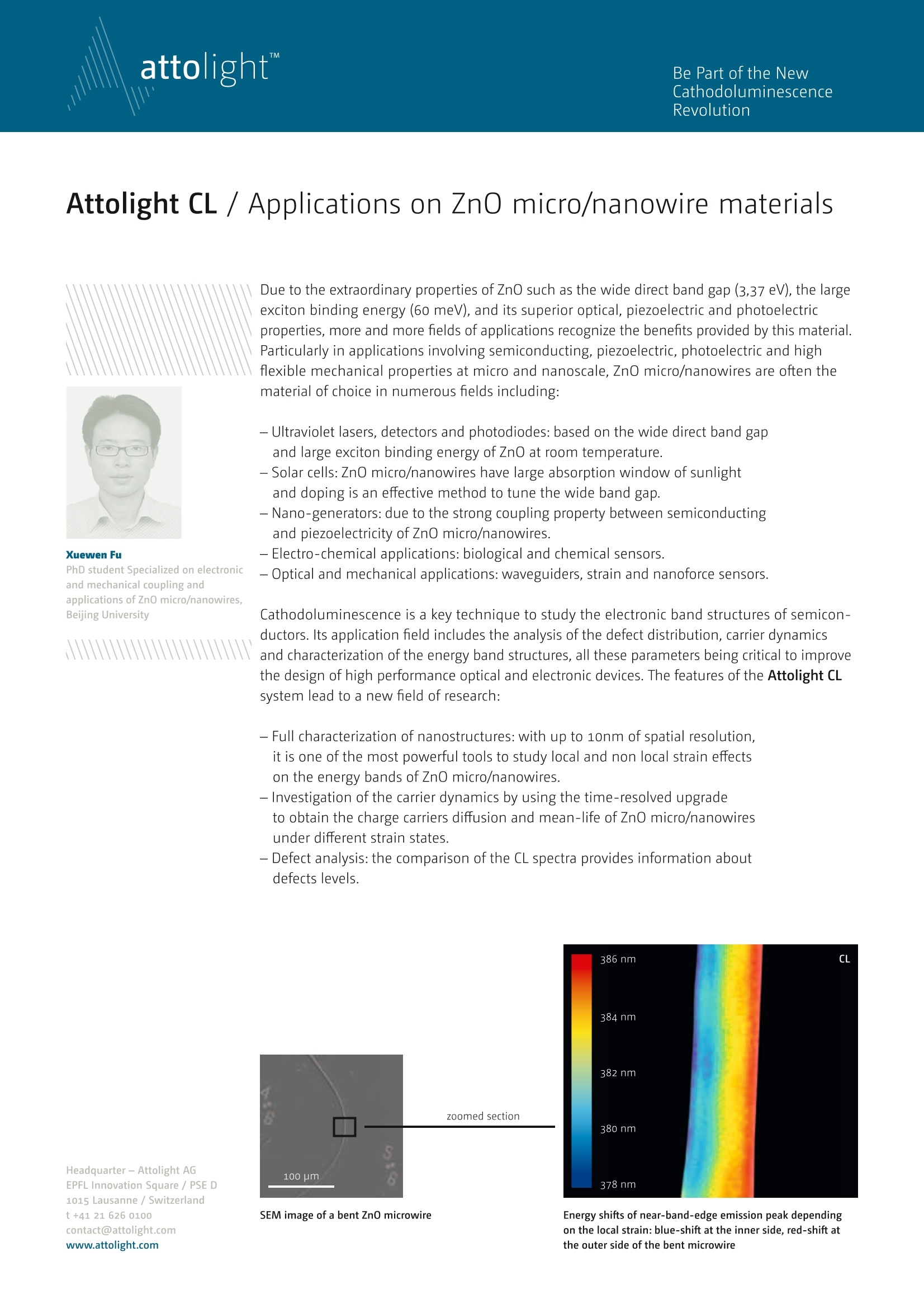
由于ZnO具有宽的直接带隙(3,37 eV)、大的激子结合能(60 meV)以及优异的光学、压电和光电性能等特性,越来越多的应用领域认识到这种材料所带来的好处,特别是在涉及半导体、压电、光电和微纳米级高柔性机械性能的应用中,ZnO微/纳米线通常是许多领域的首选材料,包括:a、紫外激光器,探测器和光电二极管:基于ZnO在室温下的宽直接带隙和大激子结合能;b、太阳能电池:ZnO微纳米线具有较大的阳光吸收窗口,而掺杂是调节宽带隙的有效方法;c、纳米发电机:由于半导体之间的强耦合特性,而ZnO微纳米线具有压电性;d、电化学应用:生物和化学传感器;e、光学和机械应用:波导,应变和纳米力传感器。 阴极发光是研究半导体电子能带结构的关键技术。它的应用领域包括缺陷分布分析、载流子动力学和能带结构的表征,这些参数对提高高性能光学和电子器件的设计至关重要。Attolight CL 系统的特点引出了一个新的研究领域:1、纳米结构的全面表征:具有高达10nm的空间分辨率,它是研究局部和非局部应变效应最有力的工具之一,将对ZnO微纳米线研究带巨大影响;2、使用时间分辨升级,从而能在不同应变状态下得到ZnO微纳米线的载流子扩散和平均寿命;3、缺陷分析:对CL光谱的比较提供了缺陷级别的信息。attolightBe Part of the New Cathodoluminescence Revolution PhD student Specialized on electronic and mechanical coupling and applications of ZnO micro/nanowires, Beijing University Due to the extraordinary properties of ZnO such as the wide direct band gap (3,37 eV), the large exciton binding energy (60 meV), and its superior optical, piezoelectric and photoelectric properties, more and more feilds of applications recognize the beneftis provided by this material. Particularly in applications involving semiconducting, piezoelectric, photoelectric and high felxible mechanical properties at micro and nanoscale, ZnO micro/nanowires are ofetn the material of choice in numerous feilds including : – Ultraviolet lasers, detectors and photodiodes : based on the wide direct band gap and large exciton binding energy of ZnO at room temperature. – Solar cells: ZnO micro/nanowires have large absorption window of sunlight and doping is an efefctive method to tune the wide band gap. – Nano-generators: due to the strong coupling property between semiconducting and piezoelectricity of ZnO micro/nanowires. – Electro-chemical applications : biological and chemical sensors. – Optical and mechanical applications : waveguiders, strain and nanoforce sensors. Cathodoluminescence is a key technique to study the electronic band structures of semicon-ductors. Its application feild includes the analysis of the defect distribution, carrier dynamics and characterization of the energy band structures, all these parameters being critical to improve the design of high performance optical and electronic devices. The features of the Attolight CL system lead to a new feild of research: – Full characterization of nanostructures : with up to 10nm of spatial resolution, it is one of the most powerful tools to study local and non local strain efefcts on the energy bands of ZnO micro/nanowires. – Investigation of the carrier dynamics by using the time-resolved upgrade to obtain the charge carriers diffusion and mean-life of ZnO micro/nanowires under difefrent strain states. – Defect analysis : the comparison of the CL spectra provides information about defects levels. SEM image of a bent ZnO microwire Energy shifst of near-band-edge emission peak depending on the local strain : blue-shiftat the inner side, red-shiftat the outer side of the bent microwire
关闭-
1/1
产品配置单
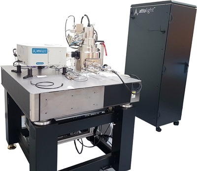
北京正通远恒科技有限公司为您提供《阴极发光设备(SEM-CL)在ZnO纳米线方面的应用》,该方案主要用于半导体材料中ZnO纳米线检测,参考标准《暂无》,《阴极发光设备(SEM-CL)在ZnO纳米线方面的应用》用到的仪器有快速定量阴极发光CL-SEM系统 Allalin。
我要纠错
推荐专场
相关方案
 咨询
咨询