方案详情文
智能文字提取功能测试中
Microelectronics Reliability 92 (2019) 149-154Contents lists available at ScienceDirect Microelectronics Reliability 92 (2019) 149-154J.-n. Wei et al. Microelectronics Reliability journal homepage:www.elsevier.com/locate/microrel Single event effects in commercial FRAM and mitigation technique usingneutron-induced displacement damage Jia-nan Wei, Hong-xia Guo,, Feng-qi Zhang, Chao-hui He *, An-an Ju",Yong-hong Li “School of Nuclear Science and Technology, Xi'an Jiaotong University, Xi'an 710049, China School of Material Science and Engineering, Xiangtan University, Hunan 411105, China State Key Laboratory of Intense Pulsed Irradiation Simulation and Effect, Northwest Institute of Nuclear Technology, Xi'an 710024, China ARTICLEINF O A B S TR ACT Keywords:Ferroelectric random access memorySingle event effectTransient micro-latch-upNeutron irradiation The single event effects (SEE) in commercial Ferroelectric Random Access Memory (FRAM) were investigatedusing heavy-ion and pulsed laser. Stable data upsets affecting one to several rows and transient data upsetsaffecting hundreds to even thousands of rows were both observed, and the corresponding sensitive regions wereidentified. Further research provides evidence that the transient micro-latch-up event in the peripheral circuitsbased on complementary metal oxide semiconductor (CMOS) process is a main cause of the transient data upsets.Moreover, neutron irradiation is performed in order to mitigate the upsets caused by transient micro-latch-up.Due to the reduction of the current gains of the parasitic bipolar transistors by neutron-induced displacementdamage, transient micro-latch-up as well as the resulting data upsets was suppressed. 1. Introduction Ferroelectric random access memory(FRAM) is a type of non-volatile memory that uses ferroelectric material such as lead zirconatetitanate (PZT) and barium strontium titanate (BST) as its storagemedium [1]. Ferroelectric material has bistable polarization stateswhich can be switched by the external electric field and can also beretained in the absence of the field. Therefore the binary information“0”and“1”can be stored by the two polarization states. In a memorycell of commercial FRAM, data is stored in a capacitor that uses fer-roelectric material as dielectric. When the data is to be read out, anexternal field is applied on the plate of the capacitor to generate thepolarization reversal current. Then a current-sensing circuit figures outthe stored data by judging the amplitude of the polarization reversalcurrent. Comparing with conventional nonvolatile technologies likeEEPROM and Flash, FRAM features high read/write speed, unlimitedendurance cycles as well as low power consumption [2]. Besides, fer-roelectric material is reported to have good resistance to radiation[3-7]. Therefore FRAM has great potential to be used in aerospace. Microelectronic devices working in the space environment willsuffer multifarious radiation effects among which single event effect(SEE) is becoming more and more serious due to technology scaling[8,9]. Some work has been done to see the SEE responses of FRAM. Theexisting results show that the memory cells based on ferroelectric ca-pacitors are immune to SEE, while the peripheral circuits are sensitive to single event upset (SEU) and single event latch-up (SEL) due to theuse of standard complementary metal oxide semiconductor (CMOS)process [10-15].Besides, various failure modes have been observed inthe peripheral circuits of commercial 130 nm FRAMs, which makes theanalysis of the experiment results more difficult [16]. Up to now, theunderlying mechanisms concerning how the perturbations in peripheralcircuits originate and how they contribute to the overall SEE responseof FRAM are not very clear. In this work, heavy-ion and pulsed laser micro-beam were used toperform SEE experiments on commercial 90 nm FRAMs from CypressSemiconductor. The four main purposes include: 1) to make furtherinvestigation on the SEE in the peripheral circuits of FRAM and classifythe upset types; 2) to identify the sensitive function blocks or regionsfor different upset types; 3) to find the main cause of the upsets andprovide experimental evidence; 4) to provide a possible post-processinghardening method to mitigate upsets in commercial-off-the-shelf(COTS) FRAM. 2. Experimental details 2.1. Device description The device under test (DUT) is FM28V100, a 1 Mbit asynchronousFRAM from Cypress Semiconductor. The FRAM array is organized as16,384 rows and each row has 8 column addresses (words). More ( E-mail a ddress: h e chaohui @ xj t u . e d u .c n (C . -h. He). ) ( ht t p s :// doi.org / 1 0.1016/ j .micr o rel.2018.1 2 .004 ) ( Received 21 August 2018; Received in revise d for m 5 November 2018; Accepted 5 December 2018 ) ( 0026-2714/C 2018 Elsevier Lt d . All rights r eserved. ) Fig. 1. Schematic diagram of the SEE test system. 2.2. Heavy-ion and pulsed laser experiment setup The setup of the SEE test system is shown in Fig. 1. The digital testermainly consists of a slave microcontroller, a DUT controller im-plemented through a FPGA and a level conversion module. The slavemicrocontroller receives test commands from the master computer toconfigure the memory controller and upload test results. The DUTcontroller is responsible for the access to the DUTs and data processing.The level conversion module is responsible for the conversion of dif-ferent logic levels to better the system's universality. The PCB card onwhich three DUTs were soldered is connected to the tester throughribbon cable. Checkerboard test pattern (55H) was written into theDUTs before the beam was turned on. This test pattern is one of themost commonly used patterns in RAM testing. The data“0”and“1”arealternately written into the memory cells. Comparing with the all“0”,all“1”or diagonal pattern, this pattern can better detect both“0”to“1”and“1”to“0” errors. In addition, this pattern is not likely to miss errorswith 00H and FFH patterns, which are frequently triggered by latch-upand single event functional interrupt (SEFI) events. DUTs were testedunder dynamic mode. Data was read out cyclically and then comparedwith the correct data to count errors. The duration of one read cycle isabout 65 ms and the interval between two read cycles is about 1 s. Thedetected errors were not corrected in order to see if they can recoverspontaneously in the following read cycles. Due to the limited spot sizeof the ion beam, only one DUT was tested in a typical test run. The heavy-ion experiment was conducted on the Heavy IonResearch Facility in Lanzhou (HIRFL) at Institute of Modern Physics,Chinese Academy of Sciences. The chosen heavy-ion is 209Bi with en-ergy of 6.1 MeV/nucleon. The experiment was performed in the air atroom temperature and the ions were at normal incident. The distancefrom the ion extraction window to the DUT was about 4 cm. The energyloss in air calculated using Geant4 is about 47%. The range in silicon ofthe ions that reach the surface of the DUT is 43 um and the LET is about99 MeVcm²mg. The DUT has five metal (copper) layers and thethickness of all the overlayers is about 5 um, while the range of atte-nuated ions in copper calculated using SRIM is 17 um. Therefore theions have enough ability to penetrate the overlayers and deposit energyin the sensitive region. The flux of ions varied from 4×10cm-2s-1to 6 ×10°cm-2.s-1 and about 260 to 390 ions struck on the DUT persecond. The totalffluence for each measurementwas about1×10°cm2. Before experiment all DUTs were decapped to exposethe die. Fig. 2 is the front side picture of the decapped FM28V100. Wecan identify the memory array (region A), decoder (region B) and senseamplifier (region C) through preliminary reverse engineering. Otherparts of the peripheral circuits such as control logic, address latch and Fig. 2. Front side picture of FM28V100. data buffer belong to region D. In order to make supplements to the heavy-ion results and distin-guish the SEE responses of different function blocks, pulsed laser ex-periment was performed on the pulsed laser micro-beam facility atNorthwest Institute of Nuclear Technology. The facility uses a picose-cond solid-state laser PL2210 (modelPL2210-SH-CX-PC), manufacturedby EKSPLA Co., Vilnius,Lithuania. The incident laser beam is focusedby a ×100 microscope objective lens and the spot diameter is about1.4 um. The DUT is placed on a three axes motorized stage. The incidentposition is determined by the coordinates of X-and Y-axes, while thefocusing of the laser on DUT is adjusted by moving the stage along Z-axis. The chosen laser wavelength was 1064 nm. To avoid the blockingof laser by the metal overlayers, the backside testing method was used.The device was decapped from backside and the silicon substrate wasthinned to about 110 um. What needs to be considered here is that if thebeam is focused on the surface of substrate, it will naturally divergealong its optical path so that the spot size at the active region may belarger than the minimized value. A shift of the stage following the z axisis confirmed to be an effective way to settle this problem [17]. Thecoordinate to focus on the active region is given by where zo is the coordinate to focus the beam on the surface of substrate,z1 is the coordinate to focus on the active region, e and n are thethickness and refractive index of the thinned substrate. Based on the backside testing method above, laser scanning wasperformed on theewholeedie area. Thelaser fluence was2.5 ×10 pulses/cm’ for each run. Test pattern and operating mode ofDUTs were identical to those in heavy-ion experiment. In addition, the Fig.3. Bit error number recorded in a typical run of heavy-ion test. supply current of the DUT was monitored by an oscilloscope through a10 sampling resistor. The trigger level was set to 400 mV. . Results and discussions 3.1. Heavy-ion results During the heavy-ion experiment, no typical SEL event occurred.The data upsets occurred in two forms: stable upsets, which would notrecover in the following read cycles, and transient upsets, which oc-curred only in one read cycle and then spontaneously recovered in thenext cycle. Fig. 3 shows the bit error number recorded in a typical run,each column represent the bit error number during a single readout ofthe DUT. The number of the upsets in a transient event is much largerthan the stable upsets, which will lead to serious reliability issues. Thecross section of the stable upsets is 1.5×10⁻³cm2. Yet considering therestorability of the transient upsets, we use transient event cross sectioninstead of upset cross section to represent the susceptibility of the DUTto transient readout failures. The calculated transient event cross sec-tion is 2.1 ×10⁻⁵cm². In order to facilitate the presentation of the results, the two kinds ofupset data are arranged as chronological bitmaps on which the ad-dresses are placed in the order of access during the test, as is shown inFig. 4. The 128 k addresses are organized as 16 k rows and each row has8 columns. The Y-axis corresponds to the row number and the X-axiscorresponds to the column number. During the test, the data in the DUTis read out row by row from 0 to 16,383. Within each row, the 8 col-umns are also read out column by column from 0 to 7. Only when the 8columns are read out successfully will the test system access the nextrow. The I/O legends correspond to the 8 data lines in the DUT's pinouts, and the I/O legends are arranged as part of the columnstructure within the bitmap. Noting that the addresses used here refer tologic addresses, the adjacent addresses in the map may be not adjacentin the memory array. The stable upsets can be classified into two categories: Type 1: The 8 words in a single row are either entirely corrupted(type 1a) or partially corrupted (type 1b). The error pattern of thecorrupted words seems to be random. Type 2: This type affects several random rows at the same time, butthe error mode inside the single rows is same as type 1 upsets. Besides,type 2 upsets usually occur right after the transient upset events. The transient upsets are termed type 3 in Fig. 4. A transient upsetevent involves hundreds to even thousands of consecutively-accessedwords, which start and stop at random address positions. This kind ofupset resembles that observed in 130 nm FRAM [16]. The difference isin the error pattern. In 130 nm FRAM, the upset pattern is reported tobe random, while only several upset patterns are observed in a transientevent in this work and one certain pattern covers consecutive wordsinstead of randomly distributing in the corrupted words. Since thetransient upsets disappear spontaneously, the ferroelectric cells are notcorrupted. Perturbations in the peripheral circuits may be involved toexplain this. In previous publications, similar large scale readout errorsin RAMs are assumed to be function failure caused by micro-latch-upevents in the readout circuits or data buffer [18]. In general, a micro-latch-up event in localized region can induce an increase of the supplycurrent, and subsequent events in other regions lead to further increasesif no power cycle is performed [19]. However, no visible increase of theDUT's supply current was observed after the heavy-ion radiation in thiswork, indicating that some other mechanisms may be involved to lib-erate the DUT from latch-up condition. 3.2. Pulsed laser results The results of the pulsed laser experiment may provide more de-tailed information. The laser energy range in this experiment is 0.1 nJto 2nJ. All upset types depicted in the heavy-ion results can be ob-served in statistically significant amounts at 0.5 nJ. For the sake ofconciseness, the analysis below is based on the results at 0.5 nJ unlessotherwise stated. During the experiment, no upset was recorded when scanning thememory array. This reconfirms the inherent tolerance to high energyparticles of the memory cells. Type 1 stable upsets were recorded inregion B, C and D, while the type 2 stable upsets and transient upsets(type 3) were recorded only in region D. According to the sensitive regions obtained from the pulsed laserresults, three hypotheses could be used to explain the type 1 stableupsets. The first is an upset in the row decoder, so the 8 words in thetarget row are not normally accessed and no switch current generatedby the ferroelectric capacitor is conducted to the input of the sense Fig. 4. Chronological bitmaps of the recorded upsets. Time (us) Fig. 5. Waveforms of the supply current transients. Zero point of the X-axiscorresponds to the trigger time. amplifier. As a result, the amplifier outputs wrong data. The second isthat a failure occurs directly in the sense amplifier, which leads to thesame errors since the 8 words in a row may share the same amplifier.The third is a failure in the control logic and access state machine, sothat the read-out or write-back signals do not match accurately [13]. Type 2 stable upsets have similar error mode inside single rows totype 1. Therefore several peripheral elements that are responsible forthe type 1 upsets in region D may be affected at the same time.Considering the fact that type 2 upsets occur right after the transientupset events, they may share some common origins with the transientupsets. Now we focus on the mechanism of the transient upsets. By mon-itoring the supply current of the DUT through an oscilloscope, wecaptured transients of the supply current which always occurred syn-chronously with the transient upsets. Fig. 5 shows several typical wa-veforms of the supply current transients. The peak value of the tran-sients is about 50 mA, which is well beyond the normal value (7mA atdynamic mode) of the DUT but not as high as a typical latch-up event.This current value does resemble the current value of the micro-latch-up event [20]. However,these current transients are quickly suppressedin 0.5us. Since we performed no power cycle during the test, the re-covery of the current could be attributed to the operation principle ofFRAM. Fig. 6 shows the timing diagram for a read access of FRAM. Aswe know, the readout of ferroelectric memory cell is destructive be-cause a positive voltage pulse is applied across the ferroelectric capa-citor to generate the switch current. Thus a precharge operation isneeded to restore the original data on the bit line back into the memorycell, so the memory is prepared for a new access [21]. The prechargeoperation is initiated by driving the chip enable (CE) signal to an in-active state. This can also put the memory into a low power or standbymode of which the typical current is only 90 uA. Due to this lowpowering scheme, the holding voltage for high current pass inside theparasitic bipolar structure is relieved so that the latch-up will not sustain. During the experiment, the operating frequency of the DUT is2MHz, so the cycle time is 0.5 us for each read operation. This isconsistent with the longest duration of the current transients. Considering the build-up time of a micro-latch-up event takes onlytens of nanoseconds, the latch-up has sufficient time to propagate be-fore it subside [20]. This kind of high current event may lead to tem-porary functional interruption and metastability of the readout circuitsor data buffers, so readout errors can cover a large amount of words.Besides, the propagation of high current events may also affect severaladjacent peripheral elements that are related to the stable upsets andresult in stable upsets in the following read cycle. This may explain thetype 2 stable upsets. As a conclusion, we judge that the current transient caused by re-storable micro-latch-up event is the origin of the transient upsets. Basedon this, some methods can be tried to mitigate the upsets by suppressingthe micro-latch-up event. 4. Mitigation technique 4.1. Basic theory The basic mechanism of micro-latch-up is similar to that of typicalSEL. The P-N-P-N structure in CMOS process brings into being theparasitic NPN and PNP transistors which may be triggered by incidentparticles, forming a positive feedback loop. Finally a low resistance andlarge current path between VDD and GND is established. In previousstudies, latch-up mitigation methods using displacement damage in-duced by high energy particles such as neutrons, protons and heavy-ions have been put forward [22-25]. By collisions of the incident par-ticles with the silicon nucleus and by collisions of the recoil primarysilicon atom with nearing atoms, interstitials and vacancies are pro-duced. After the initial recombination, remaining interstitials and va-cancies will diffuse and finally form stable defect complexes. Thesedefects can serve as effective trapping and recombination centers of thecarriers. As a consequence, basic electric properties of silicon such asthe minority carrier lifetime, the majority carrier density and the carriermobility will be influenced. The minority carrier lifetime which can bereduced significantly by displacement damage has been proved to bethe most sensitive parameter [26]. For the parasitic bipolar transistors,the reduction of the minority carrier lifetime will lead to a drop of thecurrent gain B. Let the current gain of the parasitic NPN and PNPtransistor be Bn and B, respectively, if their product (BB,) is less thanunity, the feedback loop will not be triggered so that the latch-up issuppressed. In this work, we made the attempt to use neutron-induced dis-placement damage to mitigate single event upsets caused by micro-latch-up events. The quantitative relationship between the minoritycarrier lifetime and neutron fluence is usually given as: where tro is the minority carrier lifetime before neutron irradiation, tr isthe minority carrier lifetime after neutron irradiation, K, is the coeffi-cient of radiation-induced alteration of minority carrier lifetime, D isthe neutron fluence [27]. 4.2. Neutron irradiation Neutron irradiation was performed at the fast burst reactor of theXi'an Pulsed Reactor (XAPR), China. A total of six DUTs in two groupswere used. One group was irradiated by neutrons, and the 1MeVequivalent fluence was 5 × 1013cm-2. The other group served as acontrol. DUTs were put in a cube which uses boron carbide coated bylead as shieldingnmaterial. Then/yvalueisnolessthan6.1×10°cm-rad (Si)-1 inside the cube. All devices were irradiatedunbiased with shorted terminals at room temperature. Fig. 6. Timing diagram for a read access of FRAM. Table 2 DC and AC parameters of the DUTs with (1#, 2#, 3#) and without (4#, 5#, 6#) neutron irradiation. Symbol Parameter Units Max 1# 2# 3# 4# 5# 6# IDD VpD supply current mA 12 1.3619 1.3350 1.4629 1.3975 1.4053 1.3741 IsB Standby current-CMOS uA 150 79.1960 80.1221 91.7544 91.2548 86.6442 81.6353 tAA Address access time ns 90 19 20 18 18 18 18 tcE Chip enable access time ns 60 53 52 51 51 52 52 toe Output enable access time ns 15 8 7 8 7 7 7 Fig. 9. Cross section of stable upsets before and after neutron irradiation. Fig.7. Distribution of the current transient duration before and after neutronirradiation. Energy (nJ) Fig. 10. Cross section of transient upset events before and after neutron irra-diation. Fig. 8. Bit error number recorded before and after neutron irradiation under0.5 nJ laser irradiation. 4.3. Mitigation results After neutron irradiation, functional verification was done to seewhether the devices can operate normally. Then pulsed laser experi-ment was performed again to find out the differences between the twogroups. The experiment setup was same as that depicted in Section 2.2. Functional verification was done after neutron irradiation, all DUTscould operate normally. The DC and AC parameters of the DUTs withand without neutron irradiation were measured using large scale digital integrated circuit tester. The results are partially shown in Table 2.None of the measured parameters was degraded by neutron irradiation.This is not unexpected. On the one hand, the peripheral circuits arebased on majority carrier devices (MOSFETs), the performance ofwhich is more affected by the majority carrier density and carriermobility. However, these two parameters are not significantly altereduntil the neutron fluence reaches 1 × 1014cm-²[28]. On the otherhand, the ferroelectric cells also have a neutron irradiation tolerance upto 1×1015cm-2[7]. Fig. 7 shows the distribution of the duration of the current transientsinduced by 0.5 nJ laser before and after neutron irradiation in a typicalrun. The number of current transients drops from 91 before neutronirradiation to 20 after neutron irradiation. This drop is dominated bythe decrease of transients whose duration is longer than 0.34 us.Moreover, no transient whose duration is longer than 0.38 us wascaptured after neutron irradiation. Thus a smaller scale of upsets couldbe expected for neutron-irradiated DUTs. Fig. 8 shows the bit errornumber recorded in a typical run before and after neutron irradiation at0.5 nJ. Obviously, after neutron irradiation, fewer transient events arerecorded and fewer bits are corrupted in a single transient event. Thecross sections of stable upsets and transient events before and afterneutron irradiation under different laser energies are shown in Figs. 9and 10. The cross sections of both the two kinds of upsets have a sig-nificant drop after neutron irradiation. Above all, neutron irradiation could be an effective post-processinghardening technique to mitigate single event upsets caused by transientmicro-latch-upevents in this type of FRAM. Here it is worth noting thatthe effectiveness of this method may be not always in proportion to theneutron fluence. At high neutron fluences when the majority carrierlifetime and carrier mobility begin to decrease, the well and substrateresistances will increase significantly which in turn makes the DUTmore sensitive to micro-latch-up events. This will compete with theimpact of reduced current gains. Therefore it is reasonable to judge thatan optimum neutron fluence at which the mitigation reaches saturationexists. 5. Conclusion The SEE response of 90 nm COTS FRAM was investigated usingheavy-ion and pulsed laser. Transient upsets as well as two types ofstable upsets were observed. The transient upsets involving a largeamount of words can lead to serious reliability issues if the FRAM is tobe used in radiation environment. The general sensitive region for eachtype of the upsets was identified by pulsed laser and some relatedmechanisms are discussed. The transient micro-latch-up event in per-ipheral elements such as the read out circuits and data buffers isidentified to be the main reason of the transient upsets. Moreover, thetransient high current event could also cause stable upsets. Therefore,the suppression of micro-latch-up event is crucial to the mitigation ofSEUs in FRAM. Neutron irradiation is also performed to study the impact of dis-placement damage on the transient micro-latch-up as well as the upsetscaused by it. The results show that after neutron irradiation with afluence of 5 ×1013cm-2, the number of transient micro-latch-upevents decreases sharply and the duration of the transients tends to beshorter. As a consequence, the cross sections of both transient upsetevents and stable upsets decrease a lot, indicating that neutron irra-diation may be a feasible post-processing hardening method for COTSFRAMs that are sensitive to upsets caused by micro-latch-up events. Acknowledgments This work was supported by the National Science Foundation ofChina (Grant No. 11775167). ( [1] T . E s hita , T . Tamura, Y. A r i m ot o, F err oe l ec t r i c r a n d om a c ces s m em ory ( F RA M )device s, Adv a n c es in N o n-vola t ile Me m o ry a n d S t orage T e c h nology,El s evi e r, 2 0 14, p p . 4 3 4- 4 5 4 . ) ( [2] H . I s h iwa r a, F erro e le ct ric r an d om a cces s m em o ries, J . N anosc i . N a n ot e ch n ol. 1 2 ( 10) (2012)7619- 7 627. ) ( [3] B . L i u , Y . M a, Y . Z ho u , J . L i, N e u tr on r a d i a t i on ef f e c ts i n B i 3. 1 5 N d o.8 5Ti g O 1 2 fe r r o - e lectr i c t h i n film ca p ac i to r s , R ad i a t. E f f . Defec ts So lid s 16 8 ( 2) ( 2 013 ) 1 1 5-120. ) [4] J.F. Scott, C.A. Araujo, H.B. Meadows, L.D. Mcmillan, A. Shawabkeh, Radiation ( e f fe c t s o n f e r r o e l e ct r i c thin-f i l m me mo ries : r e t e n t ion f a i l ur e m ec han i s m s, J. A p p l . P hys . 6 6 (3) (19 8 9 ) 1444-14 53 . ) ( [ 5] J .F. S cott, C .A . A r au jo, L .D. Mc Mi l la n , Ra diation dam a ge in fe rr o e l ectric thi n -f i l m m em o r i es , F e r r oelectr i c s 1 1 6 ( 1) ( 1 991) 1 0 7-1 1 0. 23 ) ( [6] J . R. S chwank , R . D . Na s by, S .L. M i l l er , M . S . R o d g e r s , P .V . Dr e sse ndo r f er, T ot a l -d o s e r adia t ion- i nd uce d de g radat i on of th i n fi l m f e rroelec t ric c a pacitors, I E E E T r a n s . N ucl. Sci . 37 (6) (1990) 170 3 - 1 712. ) ( [7] | R .A. M o or e, J. M. Benedet t o , J . M. McG a r r ity, F .B. McLean, N eu tr o n i r ra d ia t i o n e f- f ec ts on PZT t hin f ilms fo r nonv o l at i l e - mem o ry a pp l ica t ions, I EEE T r a ns. N uc l . Sc i 3 8 ( 6 )( 1 991 ) 1078-1082. ) ( [8] 1 F . I r o m , D .N. N g u y e n , M . L . U n de r w ood , A . V i r t a n en I rom, Effe c t s of s c a l i n g i n S E E a n d T I D r e s p onse o f h ig h densi t y N AND f l a sh me mori e s, IE E E Tr a ns . Nu c l . S c i . 5 7 (6 ) ( 201 0 ) 33 29- 3 335. ) ( [9] N . E. L o u r e n co , Z .E. Fl ee t wood, A . I l d e fonso , M . T . W a c h t e r , J.H . R och e , A . Kha c hatr i an, D. C m orrow , S .P. B uchner, J . H . W arner, H . I tsuji , The im p act of t e c hnol o g y s c al i ng o n t h e s i ngl e -e v e n t t ran sient r e s p onse of SiGe H B T s , IEEE Tra n s . N u cl . S c i . 64 ( 1 ) ( 20 1 7) 4 0 6 - 41 4 . ) ( [10] 1 L . Z. Scheic k , G.M . S w i f t , S . M . Gu e r t i n , S E U e valu a ti on o f S R A M me mor i e s f or space a p p lications, I E EE N ucle a r and S pa c e R ad i ation Ef f ects C on fe r ence, 20 02, p p. 6 1 - 63. ) ( [ 1 1 ] T . N u n s, S . D u z e ll ie r, J . Bertrand, G. H ubert , V . P ou get , F . Dar ra cq , J.P . Dav id , S . So o nck i ndt, E v a l uatio n o f r ec e n t tec h nolo g ie s of n onv o lat i le RAM, I E E E T r ans. N u cl . S c i . 5 5 (4 ) (200 9 ) 198 2 - 1 991 . ) ( [12] Z 2 . Z h ang , Z . L e i, Z . Y a n g , X . Wa n g , B . W an g , J . L i u , Y . E n , H . C h en , B. L i, Si n gle e vent ef fects in COT S f erroe l e c tri c RAM t e ch nologies, Radi a tion Ef fects D a ta Wor kshop (RED W ), 2 01 5, pp. 1 - 5 . ) ( [ 13]V . G u p t a , A . Bo s ser, G . T s i l i g i anni s , A. Zad e h , A . Ja va naine n , A . V i rta n en , H . P u c hner, F . S a i g ne, F . W r obel, L . D i l illo, H e a vy- i o n ra d iat io n i m p act on a 4 M b F R A M under differ e nt test mo d e s a n d co n ditions , I E E E T r an s. N u c l. Sci . 63( 4 ) ( 20 16 )2 0 1 0 - 2 015. ) ( [ 14] F . M al o u , D. D angl a , A. R ouss e t , F . X . G u erre, C o mpendiu m o f T I D and SE E t e s tr esults for v a ri o u s c a n dida t e s pa c e c r af t e l ec t ronics, E u ropea n C o nfer e n c e o n R a d ia t i o n a n d It s E f f e c ts o n C omp o ne n t s a n d S y stem s , 2 0 1 2, p p . 8 6 3 - 870. ) ( [ 15] M . V. O' B ryan , H . S . P o i v e y , S. D . K niffi n , S . P . Buc h ner , R . L. L a d b u r y, T.R . Old h a m , J . W . H owar d ,K . A . L a b e l , A. B . S a n d ers , M . B e rg , C ompen d i u m of rec e n t s i n g l e ev en t e ffec ts r e sul t s fo r c a nd ida t e s p a ce cr a f t e l ec tr o nic s fo r N A S A , Ra d i at i o n E f fects D at a Wor k shop, 20 08, p p . 1 1 - 20. ) ( [16 ] A .L. B os s er, V . G u p t a, A . Jav a n a inen , G . T s ili g ianni s, S. D. LaLumondie r e , D. Bre w e , V . F er le t -C a vr o is , H. P u c hn er, H . K e ttune n , T. G i l , F . W rob e l , F . S aig n e , A . V irtane n , L . D i li l l o, Single-e v ent effec t s in t he p eripheral circu i t ry o f a c o mme r cial f e r r o- e le c tric rando m -a c ces s m e mory , I E E E T r a ns. Nu c l . Sc i . 9 9 (20 1 8) 1 . ) ( [ 17] F . D arr a c q , H . L a pu y a de , N. B u ar d, F . M o unsi, B a c k s i d e SE U l as e r t es ti n g f o r c o mmerci a l o f f - t he- s he l f SR A M s , I E EE T ra n s. N u c l. S c i . 49 ( 6 ) ( 2002) 2977- 2 9 8 3 . ) ( [18]G . T si l igiannis, L . D i l ill o , A . Bo si o , P . G i r ard , S . P r avossoudovi t c h, A. T o dr i , A . V i r a z el , H . P u ch n er, C . Frost, F. Wr obel, F. S a i gne, Mu l t iple cel l up s e t class if i- c a t i o n in co mmer cial S RA M s, I E E E T r ans . Nu cl . S c i. 6 1 ( 4 ) (20 1 5 ) 1 7 4 7- 1 75 4. ) ( [19] D . M c m o rrow, S . B u chner, M . B a ze, B. B a r t hol e t, R . K a t z, M . O ' B r y an , C . Poivey , K . A . L a b el , R . L a dbury , M. M aher , F . W . Se x t on, L a s er -i nd uce d l a t ch u p s c r e e n i ng a nd m it i ga t ion i n CMO S d e vi c e s , I E E E T r an s . N u cl. S c i. 5 3 ( 4 ) ( 2 00 6 ) 18 19 -1824. ) [20]Y.H. Luo, F.Q. Zhang, H.X. Guo, Z. Hui, L.S. Zheng, D.M. Ji, C. Shen, D. Gong,W. Hajdas, Single-event cluster multibit upsets due to localized latch-up in a 90 nmCOTS SRAM containing SEL mitigation design, IEEE Trans. Nucl. Sci. 61 (4)(2014)1918-1923. ( [21] A / . S hei k holes lami , P. G . Gu lak, A s u r ve y of c i r cuit i n n o vati o ns i n fe r r o elect r ic r an d om-a c c es s m e mori e s, Pr o c . I E E E 8 8 (5) ( 2 0 00) 6 6 5- 6 66. ) ( [ 2 2] J .R. Ad a ms , R . J. S o ke l, N e u t r on irr a di a tion fo r p rev en tion o f l a tch-u p in MO S in- t e g ra t e d ci r cuits, I EE E T rans. N u cl . S ci. 26 ( 6 ) ( 1 979) 5 069-5 0 7 3. ) ( [23 ]J .K . E d d y ,J . B a r t ko, Th e p r event i o n of l a tc hu p in m i c roc i r c u i ts u si n g p ro t o n b e a m s , I E E E Trans . N u cl . Sc i. 28 ( 2)(1981) 1871 -1874. ) [24]JJ.P. Spratt, J.C. Pickel, R.E. Leadon, R.C. Lacoe, S.C. Moss, S.D. LaLumondiere, Asingle event latchup suppressM0Sion technique for COTS CMOS ICs, IEEE Trans. Nucl.Sci. 50 (6) (2003) 2219-2224. [25]R.C. Lacoe, S.C. Moss, J.V. Osborn, B.K. Janousek, S.D. LaLumondiere, S. Brown,D.C. Mayer, Neutron and proton irradiation for latchup suppression in a radiation-tolerant commercial submicron CMOS process, Fifth European Conference onRadiation and Its Effects on Components and Systems (RADECS), 1999, pp.340-345. [26]K.O. Petrosyants, M.V. Kozhukhov, Physical TCAD model for proton radiation ef-fects in SiGe HBTs, IEEE Trans. Nucl. Sci. 63 (4) (2016) 2016-2021. [27]G.C. Messenger, A summary review of displacement damage from high energy ra-diation in silicon semiconductors and semiconductor devices, IEEE Trans. Nucl. Sci.39(3)(1991) 468-473. [28] J.R. Srour, J.W. Palko, Displacement damage effects in irradiated semiconductordevices, IEEE Trans. Nucl. Sci. 60 (3) (2013) 1740-1766. Available online December The single event effects (SEE) in commercial Ferroelectric Random Access Memory (FRAM) were investigated using heavy-ion and pulsed laser. Stable data upsets affecting one to several rows and transient data upsets affecting hundreds to even thousands of rows were both observed, and the corresponding sensitive regions were identified. Further research provides evidence that the transient micro-latch-up event in the peripheral circuits based on complementary metal oxide semiconductor (CMOS) process is a main cause of the transient data upsets. Moreover, neutron irradiation is performed in order to mitigate the upsets caused by transient micro-latch-up. Due to the reduction of the current gains of the parasitic bipolar transistors by neutron-induced displacement damage, transient micro-latch-up as well as the resulting data upsets was suppressed.
关闭-
1/6

-
2/6

还剩4页未读,是否继续阅读?
继续免费阅读全文产品配置单
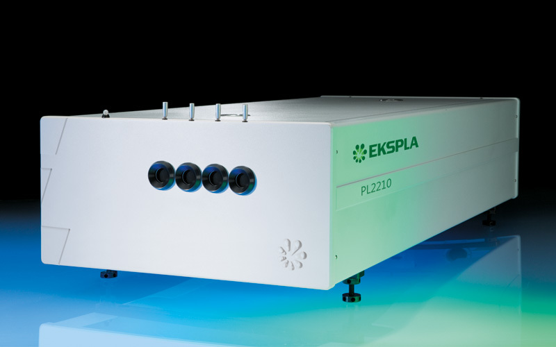
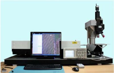
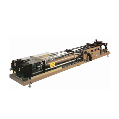
北京欧兰科技发展有限公司为您提供《商用铁电存储器(FRAM)中单粒子事件效应检测方案(激光产品)》,该方案主要用于电子元器件产品中单粒子事件效应检测,参考标准《暂无》,《商用铁电存储器(FRAM)中单粒子事件效应检测方案(激光产品)》用到的仪器有Ekspla PL2210型皮秒脉冲激光器、SPELS LSS-3 激光单粒子效应模拟测量系统。
我要纠错
推荐专场
相关方案
 咨询
咨询