
zouhua1210
第3楼2009/05/03
我先起个头.
学科领域:纳米科学与技术
专家姓名:王中林
专家国籍:美籍华人
简 介: Dr. Zhong Lin (ZL) Wang
Dr. Z.L. Wang received his Ph.D in Physics from Arizona State University in 1987, and he is a now a Regents Professor, COE Distinguished Professor and Director, Center for Nanostructure Characterization (CNC), at Georgia Tech. He served as a Visiting Lecturer in SUNY (1987-1988), Stony Brook, as a research fellow at the Cavendish Laboratory in Cambridge (England) (1988-1989), Oak Ridge National Laboratory (1989-1993) and at National Institute of Standards and Technology (1993-1995).
Dr. Wang has authored and co-authored four scientific references and textbooks, published over 530 peer reviewed journal articles, 55 review papers and book chapters, edited and co-edited 14 volumes of books on nanotechnology, and held 20 patents and provisional patents. Dr. Wang is the world’s top 25 most cited authors in nanotechnology from 1992-2002 (ISI, Science Watch). His entire publications have been cited for over 21,000 times. The H-index of his publications is 70. He is a fellow of American Physical Society and fellow of AAAS, and he has received the 2001 S.T. Li prize for Outstanding Contribution in Nanoscience and Nanotechnology, the 2000 and 2005 Georgia Tech Outstanding Faculty Research Author Awards, Sigma Xi 2005 sustain research awards, and the 1999 Burton Medal from Microscopy Society of America. He is a member of the editorial boards of over 10 major journals. He is an honorable and guest professor of over 10 universities. Two symposiums (May 7, 2003; Oct. 12, 2005) organized by the University of Pierre & Marie Curie (Paris) and sponsored by the L'Institut Universitaire de France (IUF) in the honor of Prof. Wang for his outstanding contribution in nanotechnology.
Under Dr. Wang's leadership and extremely hard work, the Georgia Tech Electron Microscopy Center was established in 1999. This Center not only links numerous research programs and groups on campus, but also is becoming a center for education and collaboration. This Center has been extensively developed and expanded to include 15 major research equipment, and it is now becomes a Center for Nanostructure Characterization and Fabrication (CNCF).
Dr. Wang is the founding Director for the Center on Nanoscience and Nanotechnology at Georgia Tech, which is playing the most crucial role in organizing GT and other universities for national competition on nanotechnology initiatives launched by federal government. Dr. Wang is also very active in initiating and driving the join research, education and degree programs between Georgia Tech and Peking University (China). He is the Chair of the Department of Advanced Materials and Nanotechnology at Peking University.
Dr. Wang’s current research focuses on discovery, controlled synthesis, characterization, fundamental understanding and applications of one-dimensional nanostructures in microsystems and biomedical science. His recent research is on semiconducting and piezoelectric oxide nanobelts for electromechanical-coupled nano-scale devices and self-assembly technology.
Dr. Wang is PI or co-PI on numerous proposals. He has received funding from NSF, DOE, DARPA, NASA, NIH China NSF and industry. The total value of contracts awarded in which he has either been PI, co-PI or an investigator is $18M over the past 13 years at Georgia Tech.
Dr. Wang is actively participating in the activities and services in scientific professional societies. He has served as chair and co-chair for 14 local, national and international conferences organized 10 symposia and chaired over 15 sessions in national and international conferences. He has served as a member for the review panel for NSF, NASA and DOE and advisory board for numerous centers on nanotechnology. He is a referee for numerous prestigious journals, such as Nature, Science, Physical Review Letters, Nature Materials and J. American Chemical Soc.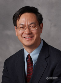
zouhua1210
第4楼2009/05/03
1. Invented nanowire piezo-electric generators for self-powered nanodevices (Science, 312, (2006) 242; Science 316 (2007) 102-104; Nature 451 (2008) 809-813)
Developing novel technologies for wireless nanodevices and nanosystems are of critical importance for in-situ, real-time and implantable biosensing, biomedical monitoring and biodetection. An implanted wireless biosensor requires a power source, which may be provided directly or indirectly by charging of a battery. It is highly desired for wireless devices and even required for implanted biomedical devices to be self-powered without using battery. Therefore, it is essential to explore innovative nanotechnologies for converting mechanical energy, vibration energy, and hydraulic energy into electric energy that will be used to power nanodevices without using battery. A groundbreaking research by Dr. Wang in 2006 is the invention of the Piezo-Electric Generators for Self-Powered Nanodevices. He demonstrated an innovative approach for converting nano-scale mechanical energy into electric energy by piezoelectric zinc oxide nanowire (NW) arrays. By deflecting the aligned NWs using a conductive atomic force microscopy (AFM) tip in contact mode, the energy that was first created by the deflection force and later converted into electricity by piezoelectric effect has been measured for demonstrating nano-scale power generator. The operation mechanism of the electric generator relies on the unique coupling of piezoelectric and semiconducting dual properties of ZnO as well as the elegant rectifying function of the Schottky barrier formed between the metal tip and the NW. The efficiency of the NW based piezo-electric power generator is ~ 17-30%.
Wang has also invented the first DC nanogenerators driven by ultrasonic wave (Science 316 (2007) 102-104). The nanogenerator is composed of aligned ZnO NWs and a zigzag top electrode, which is a novel, adaptable, mobile and cost-effective approach with a great potential in nanotechnology. The NWs can be grown on solid substrates or polymer substrates as flexible power generators. In 2008, he has developed microfiber-nanowire hybrid nanogenerator (Nature 451 (2008) 809-813), establishing the basis of using textile fibers for harvesting mechanical energy. The principle and technology demonstrated here have the potential of converting mechanical movement energy (such as body movement, muscle stretching, blood pressure), vibration energy (such as acoustic/ultrasonic wave), and hydraulic energy (such as flow of body fluid, blood flow, contraction of blood vessel) into electric energy that may be sufficient for self-powering nanodevices and nanosystems. The prototype technology established by the DC nanogenerator set a platform for developing self-powering nanosystems with important applications in implantable in-vivo biosensing, wireless and remote sensing, nanorobotics, MEMS, sonic wave detection and more.
2. Nano-Piezotronics [Adv. Mater., 19 (2007) 889]
Dr. Wang first created a field called nano-piezotronics in Dec. 2006, which utilizes the coupled piezoelectric and semiconducting properties of nanowires and nanobelts for designing and fabricating electronic devices and components, such as field effect transistors and diodes. The physics of nano-piezotronics is based on the principle of nanowire nanogenerator that converts mechanical energy into electric energy. It is anticipated to have a wide range of applications in electromechanical coupled electronics, sensing, havesting/recycling energy from the environment, and self-powered nanosystems.
3. Polar surface induced novel growth processes and mechanism of oxide nanostructures and electromechanical coupled devices (Science 303 (2004) 1348; Science, 309 (2005) 170)
The wurtzite structure family has a few important members, such as ZnO, GaN, AlN, ZnS and CdSe, which are important materials for applications in optoelectronics, lasing and piezoelectricity. The two important characteristics of the wurtzite structure are the non-central symmetry and the polar surfaces. The structure of ZnO, for example, can be described as a number of alternating planes composed of tetrahedrally coordinated O2- and Zn2+ ions, stacked alternatively along the c-axis. The oppositely charged ions produce positively charged (0001)-Zn and negatively charged (000-1)-O polar surfaces, resulting in a normal dipole moment and spontaneous polarization along the c-axis. This polar surface gives rise a few interesting growth features.
The breakthroughs by Wang’s group in 2004 is the success of first piezoelectric nanobelts and nanorings (Science 303 (2004) 1348) for applications as sensors, transducers and actuators in micro- and nano-electromechanical systems. Owing to the positive and negative ionic charges on the zinc- and oxygen-terminated ZnO basal planes, respectively, a spontaneous polarization normal to the nanobelt surface is induced. As a result, helical nanosprings/nanocoils are formed by rolling up single crystalline nanobelts. The mechanism for the helical growth is suggested for the first time to be a consequence of minimizing the total energy contributed by spontaneous polarization and elasticity. The nanobelts have widths of 10-60 nanometers and thickness of 5-20 nanometers, and they are free of dislocations. The polar surface dominated ZnO nanobelts and helical nanosprings are likely to be an ideal system for understanding piezoelectricity and polarization induced ferroelectricity at nano-scale.
The major discovery made by Wang’s group in 2005 was the discovery of a new rigid helical structure of zinc oxide consisting of a superlattice-structured nanobelt (Science, 309 (2005) 170), which was formed spontaneously in a vapor-solid growth process. Starting from a single-crystal stiff-nanoribbon dominated by the c-plane polar-surfaces, an abrupt structural transformation into the superlattice-structured nanobelt led to the formation of a uniform nanohelix due to a rigid lattice rotation or twisting. The nanohelix was made of two types of alternating and periodically distributed long crystal stripes, which were oriented with their c-axes perpendicular to each other. The nanohelix terminated by transforming into a single-crystal nanobelt dominated by nonpolar surfaces. The nanohelix could be manipulated, and its elastic properties were measured, which suggests possible uses in electromechanically-coupled sensors, transducers and resonators.
zouhua1210
第7楼2009/05/09
固体物理学家 黄昆
黄昆(1919-2005),国际著名的中国物理学家、教育家、中国固体物理学先驱、中国半导体技术奠基人。
黄昆1919年9月出生于北京,1941年毕业于燕京大学,1944年毕业于西南联合大学的北京大学理科研究所,获硕士学位,1947年在英国布里斯托大学获得博士学位。黄昆获得博士学位后曾在英国爱丁堡大学物理系、利物浦大学理论物理系从事研究工作。1951年,黄昆回到北京大学任物理系教授,1977年后任中国科学院半导体研究所所长直到退休。黄昆早年在爱丁堡大学与著名物理学家、诺贝尔奖得主玻恩教授一起从事研究工作,合著了在固体物理学界享有声誉的《晶格动力学》一书。1956年,黄昆在北京大学物理系任教授期间,参与创建了中国第一个半导体物理专业,为中国信息产业培养了第一批人材。在北京大学任教期间,黄昆还主持本科生教学体系的创建工作,并著有《固体物理学》教材,享有盛誉。1977年后,在邓小平的过问下,黄昆出任中国科学院半导体研究所所长。2001年,黄昆与其北大校友王选一同获得了该年度国家最高科学技术奖。2005年7月6日,16时18分,黄昆在北京逝世,享年86岁。
黄昆的主要荣誉包括1955年中国科学院第一批学部委员(今中国科学院院士)、2001年国家最高科学技术奖、瑞典皇家科学院外籍院士、第三世界科学院院士、全国“五一”劳动奖章获得者和1995年度何梁何利基金科学与技术成就奖获得者。黄昆还是中国人民政治协商会议全国委员会第五、六、七、八届常务委员。黄昆是中国共产党党员、九三学社社员。
黄昆的一生和诺贝尔奖大师紧密相连,从英国布里斯托大学到爱丁堡大学,再到利物浦大学,从诺贝尔奖获得者莫特教授到玻恩教授,黄昆的第一个“黄金时代”到来了。物理学大师玻恩是量子力学的创始人,也是晶体原子运动系统理论的开创者,早在第二次世界大战期间,玻恩就打算从量子学最一般原理出发,写一部关于晶格动力学的专著,但战后因忙于他事且年事已高,此事一度搁置。1947年5月中旬,黄昆来到了爱丁堡大学玻恩教授处短期工作,工作中玻恩发现黄昆熟悉这门学科,且有深邃见解,便将完成用量子力学阐述晶格动力学理论的《晶格动力学》专著的重任交给了黄昆,同时交给他的还有玻恩的一些残缺不全的旧手稿……
黄昆从1948年开始,在4年时间内不仅以严谨的论述和非常清晰的物理图像对这个固体物理学中的最基本领域进行了系统的总结,而且还以一系列创造性的工作发展和完善了这个领域。“有一段时间,我同玻恩教授还发生了争论……”谁也没想到,黄昆当初写进的内容在1960年激光发现以后,一一被实验证实。由此,奠定了他在固体物理学领域的权威地位。玻恩这位诺贝尔奖获得者也伸出了大拇指,他在给爱因斯坦的信中说:“书稿内容现在已经完全超越了我的理论……”
黄昆被选为2002年度感动中国十大人物
颁奖辞:他一生都在科学的世界里探求真谛,一生都在默默地传递着知识的薪火,面对名利的起落,他处之淡然。他不仅以自己严谨和勤奋的科学态度在科学的领域里为人类的进步做出卓越的贡献,更以淡泊名利和率真的人生态度诠释了一个科学家的人格本质。
zouhua1210
第8楼2009/05/09
纳米学界牛人 杨培东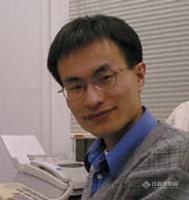
历程
1971年 出生于苏州;
1985年-1988年 就读于吴县木渎中学;
1988年-1993年 中国科技大学化学系学习。1992年获郭沫若奖学金,1993年获应用化学学士学位;
1993年-1997年 美国哈佛大学求学,1997年毕业于哈佛大学化学与生物化学系,获化学博士学位;
1997年-1998年 美国加利福尼亚大学圣芭芭拉分校从事博士后研究;
1999年至今 美国加州大学伯克利大学化学系助理教授、副教授、终身教授、教授。
期间,2001年至2004年获得美国阿尔弗雷德•斯隆奖;
2002年获得美国贝克曼青年研究员奖;
2003年被美国“技术评论”杂志列入“世界100位顶尖青年发明家”行列;
2004年获得美国材料学会(MRS)青年科学家大奖,这一奖项一年一度,只有一位获奖者,杨培东是第一位获得该奖的中国人。
2007年,美国科学基金会(NSF)授予他奖金为50万美元的艾伦•沃特曼奖,这项研究奖每年仅授予一位杰出青年科学家,在业内被称为青年诺贝尔奖。
37岁的杨培东清瘦,衣着俭朴,在独墅湖高教区的小道上碰见他,你会以为这是一个最普通不过的本科生;而在中科院苏州纳米所,进进出出他办公室的助手们则对他恭敬有加,因为这些“玩”纳米的博士和博士后最清楚,眼前这个貌不惊人的家伙曾经在这个领域里鼓捣出了些什么。
去年,美国《科学》报道了加州大学伯克利分校纳米材料学家杨培东的杰出成就。这篇题为《青云直上》的文章写道,最精细的半导体导线使杨培东大奖不断,特别是美国国家科学基金会授予他的艾伦•沃特曼奖,把他的科研生涯推向了顶峰。
“大牛”之路
纳米界流传着一个说法,如果你的博士简历上写着导师是哈佛大学的查尔斯 M.利伯教授,差不多就是在自我介绍“我是大牛”。
1993年,22岁的杨培东中国科技大学毕业后,远赴哈佛投师利伯教授门下,成为一只“牛犊”。“哈佛的四年经历,对我的学术生涯影响深远。”杨培东说,“那是我最辛苦的一段日子,光是攻克语言关,就花了两三年时间。这一关过了,学习就轻松了许多。”做科学研究,最难的是确定选题方向和制订合理的实验方案。在哈佛,杨培东最大的收获是学会了如何找出重要的科学问题,如何去解决这些问题,以及如何交叉进行多项研究任务。
全美最好的化学系在加州大学伯克利分校。1999年,在完成了18个月的博士后研究后,杨培东与大约20所美国顶尖大学面谈,最终得到近10所大学的工作邀请,他选择了伯克利,年仅28岁任职化学系助理教授。
说起来,杨培东跟伯克利还有一段故事。当年杨培东决定赴美攻博时,首选就是伯克利,然而遭到了拒绝。这一次,伯克利纠正了自己的错误。后来的事实也证明,伯克利这次做出的是一个双赢的选择。
在美国大学里,从助理教授升到终身正教授,通常要花10年左右时间。2004年,进入伯利克的第6个年头,杨培东就受聘化学系终身教授。在伯克利历史上,化学系还只聘过两位华人科学家当终身教授,前一位是诺贝尔化学奖得主李远哲博士。
认准目标,锲而不舍,这样的性格不仅体现在“择校”上,同样也体现在杨培东的科研生涯里。一进伯克利,助理教授就要独立带小组进行科学研究。良好的学术素养,加上正规的科学训练,让杨培东迅速在众多纳米技术科学家中脱颖而出,成为一颗耀眼的明星。
目前,已被公认为世界顶尖材料科学家的杨培东在伯克利带领着一个30人的科研团队,其中20人是他的博士研究生,另外10位则是博士后。今年一月,杨培东小组的又一篇论文在《自然》发表。他说,每年在顶级学术刊物上至少发表一两篇学术论文的状态已经延续了近10年。
探微之旅
从加入伯克利的那年起,杨培东就以其出色的科研成果获得了一系列殊荣。沿着一个正确的方向作始创性的研究,是杨培东频频得奖的奥秘,他的小组在半导体纳米线方面的研究,一直处在领跑这个领域的地位。
纳米技术的前景被人们一致看好。目前,世界各大公司纷纷为此项技术而斥资,几乎每一所名牌大学都以率先展开相关研究而自豪。学会如何制作纳米线这一纳米器件的关键,则成了摆在研究人员面前的一大热门课题。
顾名思义,纳米线又长又细,体积微小——大约只有人类头发宽度的万分之一。如今,研究人员能将纳米线的直径从5毫微米调整至几千毫微米,长度可达到几百微米。这种导线整合成较大的结构后,不仅可以制作激光器、晶体管和存储器阵列,就连类似猎犬嗅探器官的化学敏感结构也不在话下。
为了研制纳米线,杨培东和他的同事利用特殊的小室,先在里面将黄金或其他金属的薄膜熔化,以形成纳米尺度的微滴。然后,向它们发射化学蒸气,使其分子分解。这些分子以短序列使熔化的纳米微滴过饱和后,便形成了纳米结晶。随着更多的蒸气在金属微滴上的分解,结晶就会像一棵树那样往上生长。
同时在数百万个金属微滴上进行这一操作,使科学家有机会对大量的纳米线加以组织。杨培东“栽种”的氮化镓和氧化锌纳米线已长成大片的森林,它们能发射紫外线光,有助于“芯片上的实验室”迅速而廉价地分析医学、环境和其他取样。由于在生长过程中引进不同的蒸气,杨培东改变了纳米线的成分,使它形成硅和半导体硅锗的界面,其早期用途是对计算机芯片的冷却。此外,这类器件还有可能最终发展成为高效的能源,从汽车废热或太阳热量中产生电能。
当然,对如此细微的纳米线进行电极连接仍是一大难关,世界各地有100个研究小组正在进行攻关。
但纳米技术的应用前景实在诱人。杨培东告诉记者,他和其他四位科学家技术入股了一家纳米技术公司,他是公司科技顾问,并不直接参与经营管理。现在,这家公司正致力于将纳米技术转化到实际应用中去,已获两轮投资,烧掉了1亿5千万美元,但风投公司还是乐此不疲。
家国之恋
勤奋是杨培东最大的特质。记者采访了木渎中学八八届高三(1)班10位毕业生,当问到这位当年同班同学获得成功的最大因素时,10个人全部首选“勤奋”,其次才是天分等等。“印象最深的是,这家伙当时有一本读物《古诗一日一首》,每天宿舍熄灯后,他都要打着手电背古诗,真的是一天一首,从来不落。”一位目前从事热工研究的同学回忆道。
旅美10多年后,功成名就的杨培东依然勤奋,每天都要工作十三四个小时。在他的时间表里,工作时间从早上进学校开始,一直要持续到第二天凌晨1时左右。但其中要剔除傍晚17时到21时的4个小时,这段时间是属于女儿的。
杨培东的双博士家庭在中国留学生中很典型,妻子王玫是湖南人,也毕业于中国科技大学,在耶鲁大学获得物理学博士学位,现在旧金山市区的一家公司工作。去年夏天,杨培东把当时还只有3岁的女儿送回了国内,原因是孩子这么大的时候语言学习能力最强。3个月后回美国,小家伙果然一口普通话已经讲得特别溜。从那以后,这个在伯克利的三口之家的“官方语言”就一直是普通话。但一年下来,小家伙的普通话里偶然又要夹进些英语单词了,杨培东计划明年暑假再把她带回来“进修”一次,“尽管她生在美国,中国人的后代还是要会说中国话”。
5月12日,四川汶川大地震发生以后,杨培东更是每天关注电视新闻,灾区群众的安危与困难沉甸甸地压在他的心头。“旧金山和伯克利一湾之隔,都处在圣安德列斯断层上,属环太平洋地震带。1906年旧金山大地震后,那里的建筑都充分考虑了抗震设防要求,我工作的实验室就是建在巨大的轮子上的。”杨培东认为,四川的灾后重建,一定要多参考国外的成熟做法,提高建筑物的抗震能力。
和其他海外华人一起,他一次次参加向四川灾区捐款捐物的活动。“这次中国的抗震救灾工作信息透明,救援及时,在国际上广受好评。作为一名身在海外的中国人,我也为祖国自豪。”
醉心于探索美丽小世界的杨培东,与国内的同行,如清华大学、复旦大学和中国科技大学的研究人员保持着密切的交流。加入伯克利后,他平均每两年回中国访问一次。而中科院纳米所选定在苏州后,他回国的步伐更勤了,今年六七月,就回来了两次。“其实,纳米所还只是一片空地的时候,我就来过苏州跟他们交流了”。杨培东说,以后在苏州的工作忙起来后,回来得肯定还会更频繁。现在苏州城市大了,不自己开车总觉得不方便。“我还是中国公民,换国内的驾照应该不麻烦吧?”他问记者。
zouhua1210
第9楼2009/05/09
纳米界牛人 夏幼南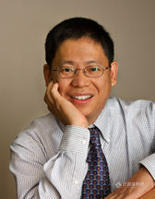
夏幼南 1965年出生,毕业于江苏省靖江中学,1982年考入中国科学技术大学化学物理系,1986年获得郭沫若奖学金,1987年获学士学位,1990年获中科院福建物质结构研究所非线性光学材料硕士学位。1991年夏幼南赴美留学,1993年,获宾州大学无机化学硕士学位,1996年获哈佛大学化学与生物化学系博士学位,师从George M. Whitesides教授,论文题目是“Soft Lithography: Micro- and Nanofabrication Based on Microcontact Printing and Replica Molding”。 96-97. 7做博士后研究,97. 7起在美国华盛顿大学化学系任助理教授,他的课题组目前承担研究项目5项,经费达32万美金。已在《Science》,《Nature》,《J. Am. Chem. Soc.》,《Adv. Mater.》等刊物上发表了50篇论文,其中第一作者24篇,其中包括在《Angew. Chem. Int. Ed.》及《Annu. Rev. Mater. Sci.》等重要刊物上发表了六篇特邀综述论文。文章发表后,引用八十余次。1997年因科研成绩突出在美国1997年在美国获Dreyfus New Faculty Award和ICI Student Award Finalist奖。主要研究领域是纳米结构材料,发明和发展了软刻技术,使用弹性材料作为模子或印章来制作纳米及亚微米结构。
主要工作创新点包括
(1)将图形化技术发展到功能高聚物的加工与应用。使用具有连续网状的管道结构的弹性模板,制备不同图形的聚合物无支撑薄膜,文章发表在《Nature》上。
(2)用弹性模子作为模板制备出多元的微米、亚微米光学表面,可用来制备具有比常规方法更小周期的衍射光栅;制备平面或曲面的有梯度的闪烁衍射光栅,其周期随位置连续改变。可以在接近半球体的表面上制备图形化的结构。可以制备正交的微透镜阵列。这些多元的图形化的微结构用其他方法难以制备。工作发表在<>上。
(3)发现了一种新的控制生长微观图形化的定向阵列的介孔(mesoscopic)SiO2的方法。该方法可以用来在非导电性的基片上制备定向排列的、具有任意微观结构的介孔管(mesoporous channels)。文章发表在《Nature》上。
(4)发展了一种新的微刻(microcontact printing)方法。将微刻技术发展到亚微米范围而不需高分辩率的光刻技术,利用反应液在固体表面可控制的活性扩展,降低通过微刻技术制得的结构的尺寸。文章发表在《J. Am. Chem. Soc.》上。软刻技术能制作的最小结构在30nm, 而目前用光刻能制作的最小结构在于250nm左右,因此这种技术可望用于末来的纳米电子元件的制作,将提供更小的,更快的三极管及其它电子元件。另外,此技术还可以用于曲面结构的制作和其他材料微加工,这对现代科学技术特别是对信息工业和微电子、光电器件的制备具有非法重要的意义。
美国化学会宣布,华盛顿大学(西雅图)化学系教授夏幼南因其在化学、物理以及纳米材料应用方面的卓越成就,荣获2005年度贝克兰奖。颁奖宴会于11月10日在新泽西州茉莉山庄的朗讯公司总部进行,夏幼南受邀出席,并在颁奖座谈会上做主题演讲。贝克兰奖用于奖励纯粹化学或工业化学的杰出成就,该奖仅包括五千美元奖金和金质奖章一枚。奖金虽微薄,奖章却成色十足,被认为美国材料化学界最高荣誉。根据美国化学会资料,夏幼南是六十年来第一位获贝克兰奖的华人化学家。
荣获贝克兰奖之前,夏幼南已获得多个学术界奖励,他1997年因科研成就获德雷福新教授奖(Dreyfus New Faculty Award);1999年,获得美国化学会拉梅尔奖(Victor K. LaMer Award);2000年,他连续获得斯隆研究奖(Research Fellow)、美国国家自然科学基金会的杰出青年教授奖(Faculty Early Career Development Award)、帕克基金会(the David and Lucile Packard Foundation)科学工程研究奖(Fellow in Science and Engineering)。
夏幼南的一位学生接受采访时称赞,夏幼南对于科研趋势有着非同寻常的敏锐,“是一位严格而仔细的教授,也是挺好的导师,特别关心学生”。夏幼南教授一直关注祖国科技发展。夏幼南作为国际著名的怀利(WILEY)出版公司出版的《Advanced Materials》编委,组织出版了该刊物的中国专辑,以五星红旗为封面,集中展示了我国材料科学前沿研究领域所取得的突出成就。2005年作为中国科大为引进依托单位的微尺度物理化学研究团队,获得中国科学院“海外知名学者”称号。
zouhua1210
第10楼2009/05/09
中国纳米界权威 张立德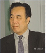
中科院固体物理研究所,1939年2月2日出生,1964年毕业于北京大学,1968年毕业于中国科学院金属研究所,获硕士学位。1987年起从事纳米技术研究,是我国最早研究纳米的科学家之一。主要研究凝聚态物理、纳米材料。他创建了中科院固体新纳米材料与纳米材料研究室和纳米材料应用发展中心,现为国家纳米科技指导协调委员会委员和技术专家、国家重点基础研究发展规划项目(973)“纳米材料和纳米机构”首席科学家、中国颗粒学会理事、超微粒子专业委员会主任、中国科学院纳米科技中心学术委员会副主任、中国材料学会理事。发表SCI收论文300余篇;获发明专利13项,已经实施四项;获国家及省部级奖励六项;已出版专著4部、编著3部,共培养博士生30余名.
并撰写了纳米材料专著《纳米材料学》、《材料新星——纳米材料》,申请专利12项,发表学术论文200余篇。现为国家纳米科技指导协调委员会委员和技术专家、国家重点基础研究发展规划项目(973)“纳米材料和纳米机构”首席科学家、中国颗粒学会理事、超微粒子专业委员会主任、中国科学院纳米科技中心学术委员会副主任、中国材料学会理事。发表SCI收论文300余篇;获发明专利13项,已经实施四项;获国家及省部级奖励六项;已出版专著4部、编著3部,共培养博士生30余名.获奖成果有:
一、晶粒间界内耗新进展,获中科院科技进步一等奖。
二、低能位错组态电镜观察,获中科院自然科学三等奖